High transmission in All-optical Logic gate formed by crystal - - PowerPoint PPT Presentation

high transmission in all optical logic gate formed by
SMART_READER_LITE
LIVE PREVIEW

High transmission in All-optical Logic gate formed by crystal - - PowerPoint PPT Presentation

High transmission in All-optical Logic gate formed by crystal photonic Y- junction DERDOUR ROUMAISSA 1 , LEBBAL MOHAMED REDHA 2 , SOUHEIL MOUETSI 1 , T.BOUCHEMAT 2 , M.BOUCHEMAT 2 1 Department of Electronics Faculty of Engineering, University of


slide-1
SLIDE 1

DERDOUR ROUMAISSA1, LEBBAL MOHAMED REDHA2, SOUHEIL MOUETSI1, T.BOUCHEMAT2, M.BOUCHEMAT2 1 Department of Electronics Faculty of Engineering, University of Larbi Ben M’hidi OUM EL BOUAGHI, Algeria 2 Department of Electronics Faculty of Engineering, Mentouri University Constantine, Algeria

High transmission in All-optical Logic gate formed by crystal photonic Y- junction

Introduction Theory Simulation Setup Results Conclusion References

[1] Ref. 1K. Sakoda, Optical Properties of Photonic Crystals, Springer-Verlag, Berlin, 2001 [2] Ref. 2Z. Wu, K. Xie, H. Yang, Band gap properties of two-dimensional photonic crystals with rhombic lattice, Optik 123 (2012) 534–536 [3] Ref. 3F. Mehdizadeh, H. Alipour-Banaei, Z. Daie-Kuzekanani, All optical multi reflection structure based on one dimensional photonic crystals for WDM communication systems”, Optoelectronics Adv. Mater-Rapid Commun 6 (2012) 527–531 [4] Ref. 4H. Alipour-Banaei, F. Mehdizadeh, A proposal for anti-uvb filter based on

  • nedimensional photonic crystal structure, DigestJ. Nanomater. Biostruct. 7 (2012) 361–367

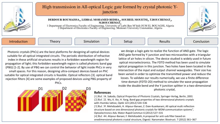
Photonic crystals (PhCs) are the best platforms for designing all optical devices suitable for all optical integrated circuits. The periodic distribution of refractive index in these artificial structures results in a forbidden wavelength region for propagation of light; this forbidden wavelength region is called photonic band gap (PBG) [1-2]. By use of PBG we can control the behavior of light inside PhCs in very small spaces. For this reason, designing ultra-compact devices based on PhC suitable for optical integrated circuits is feasible. Optical reflectors [3]. optical band rejection filters [4] are some examples of proposed devices using PBG property of PhCs. we design a logic gate to realize the function of AND gate. The logic AND gate formed by Y-junction and two microcavities with a triangular lattice of air holes in silicon. The device studied is widely used in future

  • ptical microelectronics. The FDTD method has been used to simulate
  • ptical propagation in this junction. Two holes have been located in the

intersection of the input and output channel waveguides. Their size has been varied in order to optimize the transmitted power and reduce the

  • losses. To validate our results numerically, we use a finite difference

time-domain (FDTD-2D) method to simulate the wave propagation inside the double bend and the Y-junction splitter in a two-dimensional photonic crystal,

D1 D2 D3

slide-2
SLIDE 2

Lab symbolics Lab symbolics

Introduction Theory Simulation Setup Results Conclusion References

[5] Ref. 5 Zhang, Z., Satpathy, S. “Electromagnetic Wave Propagation in Periodic Structures: Bloch Wave Solution

  • f Maxwell's Equations”, Phys. Rev. Lett. 65

THE FIELD EQUATIONS

Which in the above relationships: D(r,t)=ϵ0ϵrE⃗ (r,t) and B⃗(r,t)=μ0H⃗(r,t). In the given relations, ϵr is relative electric permittivity ϵ0 is the air permittivity and μ0 is the magnetic permittivity For the purpose of this study, we were most interested in analyzing this type of mode, considering that the forbidden band gap was apparently created for TM polarization Using the Maxwell's equations, it is possible to find the time-independent equation for the wave equation [5],

References

[5] Ref. 5Zhang, Z., Satpathy, S. “Electromagnetic Wave Propagation in Periodic Structures: Bloch Wave Solution of Maxwell's Equations”, Phys. Rev. Lett. 65

THE FIELD EQUATIONS

To study the behavior of light in photonic crystals, it is necessary to solve Maxwell's equations. Maxwell's equations consist of two main equations, those of TE and TM polarization [5].

Using the acquired equation and solving it, it is possible to calculate the optical power distribution and special frequencies in a lattice

High transmission in All-optical Logic gate formed by crystal photonic Y-junction

DERDOUR ROUMAISSA1, LEBBAL MOHAMED REDHA2, SOUHEIL MOUETSI1, T.BOUCHEMAT2, M.BOUCHEMAT2 1 Department of Electronics Faculty of Engineering, University of Larbi Ben M’hidi OUM EL BOUAGHI, Algeria 2 Department of Electronics Faculty of Engineering, Mentouri University Constantine, Algeria

(1) (3) (2) (4)

slide-3
SLIDE 3

Lab symbolics Lab symbolics

Introduction Theory Simulation Setup Results Conclusion References

[6] Ref. 6 Y. Tetsuro, G. Masahiro, K. Toshiaki, N. Kazuhiro,S. Shinnosuke, IEEE J. Quant. Electr. 38, 37 (2002)

DESIGN AND ANALYSIS

  • Fig. 2 shows the band structure for the proposed photonic crystal lattice. It has been

calculated by employing a 2D plane wave expansion method. A complete photonic band gap centered at telecommunication wavelengths can be determined.

DESIGN AND ANALYSIS

The model proposed formed by a Y-junction, which is the basic building block of integrated optics coupled with two microcavities introduced in the center of the three waveguide as shown in Fig. 1. This structure based on a triangular lattice of air holes in silicon, which has been chosen because triangular lattices may exhibit large band gaps and the silicon is expected to be a good platform for integrated photonics circuits and ultra-compact optical devices [6].

  • Figure. 1. The proposed structure for AND logic gates.
  • Figure. 2. The obtained band structure for the given photonic crystal lattice

DERDOUR ROUMAISSA1, LEBBAL MOHAMED REDHA2, SOUHEIL MOUETSI1, T.BOUCHEMAT2, M.BOUCHEMAT2 1 Department of Electronics Faculty of Engineering, University of Larbi Ben M’hidi OUM EL BOUAGHI, Algeria 2 Department of Electronics Faculty of Engineering, Mentouri University Constantine, Algeria

High transmission in All-optical Logic gate formed by crystal photonic Y-junction

slide-4
SLIDE 4

Lab symbolics Lab symbolics

Introduction Theory Simulation Setup Results Conclusion

When we add another hole at the center of the Y-junction figure 1, higher order modes are removed. The total transmission at the output ports is improved compared to the last structure this is clearly seen in (figure 4). THE TRANSMITTED IN PROPOSED ALL-OPTICAL AND LOGIC GATE

Figure 3 shows the design of an all optical AND logic gate on the platform of 2D crystal photonic. In this structure a symmetric Y-shaped waveguide is formed and a hole is introduced at the center of the three waveguides. (Figure 3 “a”). The normalized transmission obtained by 2D-FDTD is illustrated in (figure 3”b”). Figure 3: (a) Design of the Y-junction. (b) Transmission of the AND logic gate with one cavity

AFTER ADDING THE CAVITY: When we add another hole at the center of the Y-junction figure 1, higher order modes are removed. The total transmission at the output ports is improved compared to the last structure this is clearly seen in (figure 4). Figure 4:The spectral response in transmission of the all-optical AND logic gate after adding the cavity DERDOUR ROUMAISSA1, LEBBAL MOHAMED REDHA2, SOUHEIL MOUETSI1, T.BOUCHEMAT2, M.BOUCHEMAT2 1 Department of Electronics Faculty of Engineering, University of Larbi Ben M’hidi OUM EL BOUAGHI, Algeria 2 Department of Electronics Faculty of Engineering, Mentouri University Constantine, Algeria

High transmission in All-optical Logic gate formed by crystal photonic Y-junction

slide-5
SLIDE 5

Lab symbolics Lab symbolics

Introduction Theory Simulation Setup Results Conclusion

When we add another hole at the center of the Y-junction figure 1, higher order modes are removed. The total transmission at the output ports is improved compared to the last structure this is clearly seen in (figure 4). THE TRANSMITTED IN PROPOSED ALL-OPTICAL AND LOGIC GATE

AFTER OPTIMIZATION: In order to improve the transmission properties we have change the position

  • f the two cavities (Figure 5) by moving them inside the right guide.

Figure 5: Design of the optimized All-optical AND logic gate In (figure 6) the transmission is clearly increased with this new configuration, so we can conclude that the last modification proved the theoretical results who say that in crystal photonic the substitutions defects change the transmission

Figure 6: the spectral response in transmission of the optimized All-optical AND logic gate.

DERDOUR ROUMAISSA1, LEBBAL MOHAMED REDHA2, SOUHEIL MOUETSI1, T.BOUCHEMAT2, M.BOUCHEMAT2 1 Department of Electronics Faculty of Engineering, University of Larbi Ben M’hidi OUM EL BOUAGHI, Algeria 2 Department of Electronics Faculty of Engineering, Mentouri University Constantine, Algeria

High transmission in All-optical Logic gate formed by crystal photonic Y-junction

slide-6
SLIDE 6

Lab symbolics Lab symbolics

Introduction Theory Simulation Setup Results Conclusion

SIMULATION AND RESULTS SIMULATION AND RESULTS

Truth table 1 for AND logic gate, where the output signal is as a function of input power Pi show that the system performs as an AND gate. PORT A PORT B PORT C

LOGICAL OUTPUT

0Pi 1 0.017Pi 1 0.017Pi 1 1 1.038Pi 1 Table1: The truth table for AND logic gate, where the output signal is as a function of input power Pi

Figure 7 : Field distributions at steady state of the ‘‘AND'' logic gate for (a) A=1, B=0; (b) A=0, B=1 and (c) A=1, B=1.

The cavity mode whose magnetic field configuration is depicted in figure 7 needs to be coupled to one of the guided modes in the PC waveguide. The results prove that the structure suggested could really (functioned as a logical gate "AND“ using the devices optic based on photonic crystals.

DERDOUR ROUMAISSA1, LEBBAL MOHAMED REDHA2, SOUHEIL MOUETSI1, T.BOUCHEMAT2, M.BOUCHEMAT2 1 Department of Electronics Faculty of Engineering, University of Larbi Ben M’hidi OUM EL BOUAGHI, Algeria 2 Department of Electronics Faculty of Engineering, Mentouri University Constantine, Algeria

High transmission in All-optical Logic gate formed by crystal photonic Y-junction

slide-7
SLIDE 7

Lab symbolics

  • r author photo

Lab symbolics

  • r author photo

Introduction Theory Simulation Setup Results Conclusion

The most significant result are: *To increase the transmission and obtain a wide bandwidth at the output port. we have performed numerical simulations on Y-junction waveguide, and achieved an improvement of transmission by placing two microcavities in the center of the three waveguides. *We found through this study that the transmission properties are clearly improved, the propagation mode is not affected by the accident posed by the corners, allowing the wave to follow the direction

  • f bends and we have proved that the proposed structure could really function as an AND logic gate

with a highest transmission and low losses. Contacts: maroma18@yahoo,fr

DERDOUR ROUMAISSA1, LEBBAL MOHAMED REDHA2, SOUHEIL MOUETSI1, T.BOUCHEMAT2, M.BOUCHEMAT2 1 Department of Electronics Faculty of Engineering, University of Larbi Ben M’hidi OUM EL BOUAGHI, Algeria 2 Department of Electronics Faculty of Engineering, Mentouri University Constantine, Algeria

High transmission in All-optical Logic gate formed by crystal photonic Y-junction