
1.1
Spiral 0 – Review of EE 109L
Class Overview Analog to Digital Conversion Binary Representation MIPS Assembly and CPU Organization
1.2
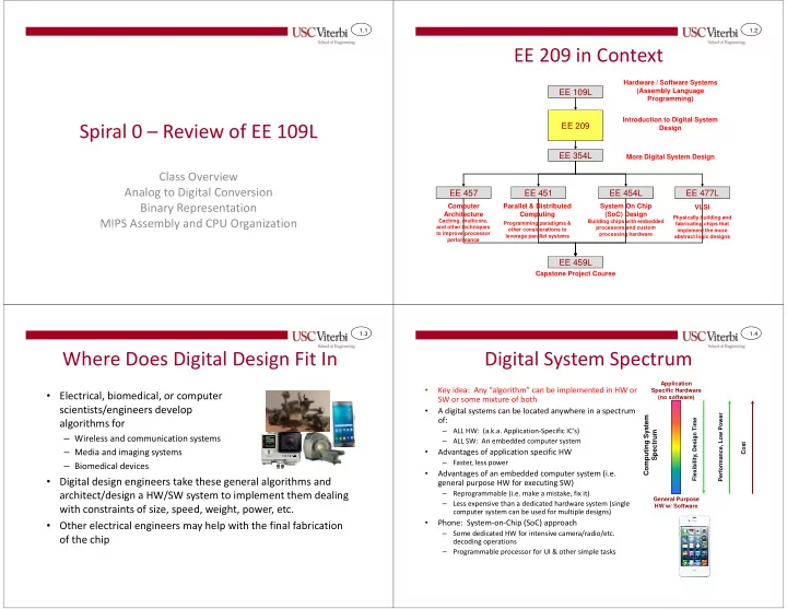
EE 209 in Context
EE 109L EE 209 EE 457 EE 354L EE 477L EE 459L
Hardware / Software Systems (Assembly Language Programming) Computer Architecture
Caching, multicore, and other techniques to improve processor performance Physically building and fabricating chips that implement the more abstract logic designs
VLSI Capstone Project Course
EE 451
Building chips with embedded processors and custom processing hardware
EE 454L
Introduction to Digital System Design More Digital System Design System On Chip (SoC) Design Parallel & Distributed Computing
Programming paradigms &
- ther considerations to
leverage parallel systems 1.3
Where Does Digital Design Fit In
- Electrical, biomedical, or computer
scientists/engineers develop algorithms for
– Wireless and communication systems – Media and imaging systems – Biomedical devices
- Digital design engineers take these general algorithms and
architect/design a HW/SW system to implement them dealing with constraints of size, speed, weight, power, etc.
- Other electrical engineers may help with the final fabrication
- f the chip
1.4
Digital System Spectrum
- Key idea: Any “algorithm” can be implemented in HW or
SW or some mixture of both
- A digital systems can be located anywhere in a spectrum
- f:
– ALL HW: (a.k.a. Application-Specific IC’s) – ALL SW: An embedded computer system
- Advantages of application specific HW
– Faster, less power
- Advantages of an embedded computer system (i.e.
general purpose HW for executing SW)
– Reprogrammable (i.e. make a mistake, fix it) – Less expensive than a dedicated hardware system (single computer system can be used for multiple designs)
- Phone: System-on-Chip (SoC) approach
– Some dedicated HW for intensive camera/radio/etc. decoding operations – Programmable processor for UI & other simple tasks
Computing System Spectrum
Application Specific Hardware (no software) General Purpose HW w/ Software Flexibility, Design Time Performance, Low Power Cost