
SLIDE 1
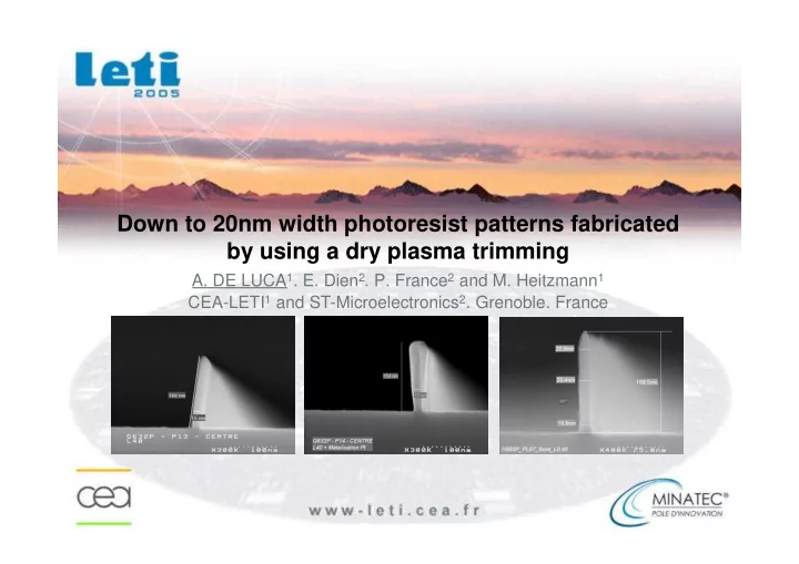
Down to 20nm width photoresist patterns fabricated by using a dry plasma trimming
- A. DE LUCA1. E. Dien2. P. France2 and M. Heitzmann1
Down to 20nm width photoresist patterns fabricated by using a dry - - PowerPoint PPT Presentation
Down to 20nm width photoresist patterns fabricated by using a dry plasma trimming A. DE LUCA 1 . E. Dien 2 . P. France 2 and M. Heitzmann 1 CEA-LETI 1 and ST-Microelectronics 2 . Grenoble. France . 2005 AGENDA Introduction Different
2
2005 AGENDA
3
2005
4
2005
10 20 30 40 50 60 70
CD Bias (nm)
O2 % in Gas Feed
10 20 30 40 50 60 70
5 10 15 Cl2 HCl HBr
O % in Gas Feed
Dense-Iso CD Bias difference (nm)
Trim rate (isolated) > Trim rate (dense) Trim rate (isolated) < Trim rate (dense)
2
CD Bias as = CD after trimming – CD before trimming
5
2005 DESCRIPTION OF THE EXPERIMENT
CD Si-Bulk HTO ~ 100 nm Ep
6
2005
Vcr (nm. S-1)
0.5 1 1.5 2 2.5 3 10 20 30 40 50 Cl2-O2 (40%) Cl2-O2 (30%)
CF4-O2 (30%) HBr-O2 (30%)
7
2005
1.5 1.2 0.9 20 HBr-O2 1.25 0.8 0.6 30 CF4-O2 1.1 0.25 0.08 120 Cl2-O2 Microloading Trim etch rate (nm.s-1) Vertical etch rate (nm.s-1) Process time (s) Chemistry 20 40 60 80 100 120 40
50
75 Cl2-O2 CF4-O2 HBr-O2
% of valid patterns Initial pattern size (nm)
8
2005
9
2005
0.85 0.15 0.8 30 1.1 0.3 0.1 40 1.3 0.35 0.185 50 Microloading Trim etch rate (nm.s-1) Vertical etch rate (nm.s-1) % of O2
10
2005
20 40 60 80 100 120 40 50 75
50% of O2 40% of O2 30% of O2 % of valid patterns Initial pattern size (nm)
11
2005
12
2005
20 40 60 80 100 20 40 60 80 100 120 140
% of valid patterns Trimming time (s)
13
2005
14
2005
15
2005
16
2005
40 40 % of O2 5 10 5 10 Pressure (mTorr) HBr Cl2-O2 HBr Cl2-O2 Chemistry 1500 300 1500 300 Ws (W) Wb (W) 60 40 60 90 Time (s) 2nd hardening 2nd trimming 1irst hardening 1irst trimming Parameters
17
2005
51.1 30.8 20.4 78.1 51.7 45.8 Mean 50.2 30.1 20 76.5 56.5 44.6 H585-P10 53.7 32.8 22.2 79.2 58.8 46.6 H585-P09 51.9 32 21.8 77.2 57.6 46.2 H585-P08 48.6 28.8 18.5 78.1 58.7 45.7 H585-P07 51.1 30.2 19.3 79.4 58.7 46 H585-P06 75 nm 50 nm 40 nm 75 nm 50 nm 40 nm Pattern size CD after trimming (nm) CD before trimming (nm)
18
2005 RESULTS AND DISCUSSION
19
2005