Development of Tiled Gamma-ray Detector Circuit using Photodetector - - PDF document

development of tiled gamma ray detector circuit using
SMART_READER_LITE
LIVE PREVIEW

Development of Tiled Gamma-ray Detector Circuit using Photodetector - - PDF document

Transactions of the Korean Nuclear Society Virtual Spring Meeting July 9-10, 2020 Development of Tiled Gamma-ray Detector Circuit using Photodetector Array Kyeyoung Cho a , Young-Jun Jung a , Jungyeol Yeom a , Hakjae Lee b , Hyemi Cha a , Kisung


slide-1
SLIDE 1

Development of Tiled Gamma-ray Detector Circuit using Photodetector Array

Kyeyoung Cho a, Young-Jun Jung a, Jungyeol Yeom a, Hakjae Lee b, Hyemi Cha a, Kisung Lee a

a School of Biomedical Engineering, Korea University, Seoul 02841, Korea b ARALE Laboratory Co. Ltd., Seoul, Korea *Corresponding author: kisung@korea.ac.kr

  • 1. Introduction

The developed sub-miniature gamma camera is a compact and lightweight device that is easy to use in various fields that require miniaturization, such as portable and wearable devices, and drone-based

  • systems. In this study, we developed an extended-type

gamma-ray detector circuit by tiling the photodetector used in the sub-miniature gamma camera and suggested the possibility of extending the gamma-ray

  • detector. Through this, we aimed to verify the

performance improvement such as the extension of the detection area and increased sensitivity. In addition, it presented the possibility of extension structure of various arrays including the square array.

  • 2. Methods and Results

In this section some of the techniques used to develop a tiled gamma-ray detector are described. The tiled gamma-ray detector is composed

  • f

a photodetector, a scintillator, analog signal processing circuits (charge division circuit, preamplifier, position encoding amplifier, low pass filter, and baseline adjustment circuit), and digital signal processing circuits (analog to digital converter (ADC) and field programmable gate array (FPGA)). 2.1 Photodetector and scintillator The tiled gamma-ray detector was composed of 8 × 8 multi-pixel photon counter (MPPC) sensors. Four MPPC sensors were arranged in a 2 × 2 tile shape and had a detection area with dimensions of 51.6 mm × 51.6 mm, as shown in Fig. 1(a). We used a CsI(Tl) scintillator, which has good light yield, low energy resolution, and low costs with no background radiation.

  • Fig. 1. Tiled MPPC array (a), and CsI(Tl) scintillator array (b)

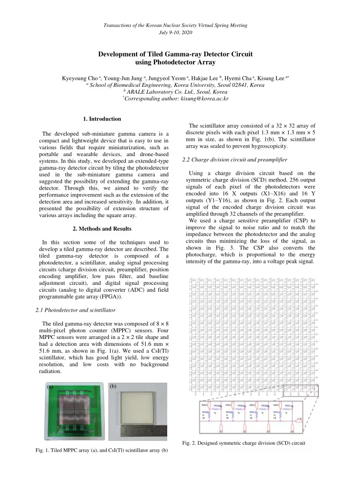
The scintillator array consisted of a 32 × 32 array of discrete pixels with each pixel 1.3 mm × 1.3 mm × 5 mm in size, as shown in Fig. 1(b). The scintillator array was sealed to prevent hygroscopicity. 2.2 Charge division circuit and preamplifier Using a charge division circuit based on the symmetric charge division (SCD) method, 256 output signals of each pixel of the photodetectors were encoded into 16 X outputs (X1–X16) and 16 Y

  • utputs (Y1–Y16), as shown in Fig. 2. Each output

signal of the encoded charge division circuit was amplified through 32 channels of the preamplifier. We used a charge sensitive preamplifier (CSP) to improve the signal to noise ratio and to match the impedance between the photodetector and the analog circuits thus minimizing the loss of the signal, as shown in Fig. 3. The CSP also converts the photocharge, which is proportional to the energy intensity of the gamma-ray, into a voltage peak signal.

  • Fig. 2. Designed symmetric charge division (SCD) circuit

Transactions of the Korean Nuclear Society Virtual Spring Meeting July 9-10, 2020

slide-2
SLIDE 2
  • Fig. 3. Designed charge sensitive preamplifier (CSP) circuit

2.3 Position encoding amplifier The purpose of a position encoding amplifier (PEA) is to encode a voltage signal of 32 channels from CSP circuits into four channel signals (X+, X-, Y+, Y-) through a summing amplifier, as shown in Fig. 4. To determine the position of the detected signals, each voltage signal from the CSP was amplified using different Rin values of the summing amplifier. Therefore, each signal had different amplitudes. The total gain of the amplifier was designed using the Rin and Rf values from the summing amplifier.

CX9 CX11 1.417k XR9 0.911k XR19 5.1k Rg2 1B CX13 0.638k XR2 2.125k XR3 CX14 0.671k XR4 1.821k XR5 10u C68 1.063k XR18 EX- CX15 0.708k XR6 1.594k XR7 0.911k XR14 1.063k XR15 0.981k XR16 1.275k XR11 5.1k Rg1 1B 1.275k XR22 0.797k XR23 CX16 0.750k XR8 CX7 0.981k XR17 0.850k XR21 1.417k XR24 0.750k XR25 1k RL2 1B 1.594k XR26 0.708k XR27 CX1 CX5 CX10 1.821k XR28 0.671k XR29 CX2 0.850k XR12 1k RL1 1B EX+

  • 3.3V

2.125k XR30 0.638k XR31 2.55kk XR32 CX3 1.159k XR13 0.797k XR10 U3 AD823an/AD + 3

  • 2

V+ 8 V- 4 OUT 1 CX4 0.1u C65 CX8 0.1u C67 U4 AD823an/AD + 3

  • 2

V+ 8 V- 4 OUT 1 CX6 10u C66 1.159k XR20 CX12 2.55k XR1 +3.3V

  • Fig. 4. Designed position encoding amplifier (PEA) circuit

2.4 Filter and baseline adjustment circuit To remove the high frequency noise, we designed an active low pass filter for output signals (X+, X-, Y+, Y- ) of PEA. The baseline adjustment circuit was applied to adjust the baseline of each signal to the -500 mV level, as shown in Fig. 5.

  • Fig. 5. Designed filter and baseline adjustment circuit.

2.5 ADC and FPGA Four channel signals (X+, X-, Y+, Y-) were converted into a digital signal through ADC. The digital signals were determined as event data by a peak detection logic circuit programmed in the FPGA. The event data provides gamma-ray energy and position

  • information. It was packaged and converted to a

UDP/IP packet communication protocol by a Nios II processor. 2.6 Experiment environment and Performance Test To verify the performance of the tiled gamma-ray detector, a flood image and energy histogram were acquired using an Na-22 standard source for one hour. A CsI(Tl) crystal array has an energy resolution of 12.92% for an energy histogram. Through the flood map image, it was verified that the CsI(Tl) pixels were clearly distinguished, as shown in Fig. 6. In addition, it was verified through the peak evaluation of the vertical axis profile that 29 pixels were distinguished. The FWHM of profile was 1.075mm, as shown in Fig. 7.

  • Fig. 6. Flood map with Na-22 standard source

Transactions of the Korean Nuclear Society Virtual Spring Meeting July 9-10, 2020

slide-3
SLIDE 3
  • Fig. 7. Profile with Na-22
  • 3. Conclusions

In this study, a tiled gamma-ray detector circuit was developed to improve performance such as the extension of the detection area and increasing

  • sensitivity. Additionally, by acquiring and evaluating an

image, the possibility of extension was verified. These results suggest the possibility of extended structures of various arrays including square arrays. Based on the results of this study, we will proceed with performance optimization of the developed circuit and conduct a study on the development of tiled gamma-ray detectors applying the extension structure of various arrays. REFERENCES

[1] Jung, Young-Jun, et al. "Development of a sub-miniature gamma camera for multimodal imaging system." Nuclear Instruments and Methods in Physics Research Section A: Accelerators, Spectrometers, Detectors and Associated Equipment (2019). [2] D. Olcott, F. Habte, C.S. Levin, A.M. Foudray, Performance characterization of aminiature, high sensitivity gamma ray camera, IEEE Symp. Conf. Rec. Nucl. Sci. 6(2004) 1492–1497 [3] Popov, V., et al. "Analog readout system with charge division type

  • utput."

2001 IEEE Nuclear Science Symposium Conference Record (Cat. No. 01CH37310). Vol.

  • 4. IEEE, 2001.

[4] J. A. Sorenson and M. E. Phelps, Physics in nuclear medicine, Grune & Stratton New York, 1987. Transactions of the Korean Nuclear Society Virtual Spring Meeting July 9-10, 2020