
SLIDE 1
Technical University Tallinn, ESTONIA
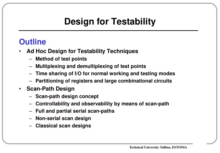
Design for Testability
Outline
- Ad Hoc Design for Testability Techniques
– Method of test points – Multiplexing and demultiplexing of test points – Time sharing of I/O for normal working and testing modes – Partitioning of registers and large combinational circuits
- Scan-Path Design