
SLIDE 1
Contents Slide 1-1 Some DSP Chip History Slide 1-2 Other DSP - - PDF document
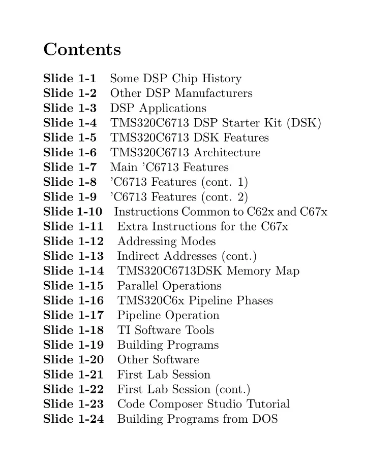
Contents Slide 1-1 Some DSP Chip History Slide 1-2 Other DSP Manufacturers Slide 1-3 DSP Applications Slide 1-4 TMS320C6713 DSP Starter Kit (DSK) Slide 1-5 TMS320C6713 DSK Features Slide 1-6 TMS320C6713 Architecture Slide 1-7 Main
MIC IN LINE OUT HP OUT LINE IN
0 1 2 3 0 1 2 3
JP1 1.26V JP2 3.3V ENDIAN BOOTM 1 BOOTM 0
32 8
8 1 3 2 Config SW3 32 HPI_EN 4
JP4 5V
functional block and CPU (DSP core) diagram
Test C67x CPU Data Path B B Register File Instruction Fetch Instruction Dispatch Instruction Decode Data Path A A Register File Power-Down Logic .L1† .S1† .M1† .D1 .D2 .M2† .S2† .L2† L1P Cache Direct Mapped 4K Bytes Total Control Registers Control Logic L1D Cache 2-Way Set Associative 4K Bytes In-Circuit Emulation Interrupt Control
C6713 Digital Signal Processor † In addition to fixed-point instructions, these functional units execute floating-point instructions.
Enhanced DMA Controller (16 channel) L2 Cache/ Memory 4 Banks 64K Bytes Total (up to 4-Way) Clock Generator, Oscillator, and PLL x4 through x25 Multiplier /1 through /32 Dividers L2 Memory 192K Bytes EMIF McASP1 McASP0 McBSP1 McBSP0 I2C1 I2C0 Timer 1 Timer 0 GPIO HPI
Pin Multiplexing McBSPs interface to: –SPI Control Port –High-Speed TDM Codecs –AC97 Codecs –Serial EEPROM EMIF interfaces to: –SDRAM –SBSRAM –SRAM, –ROM/Flash, and –I/O devices McASPs interface to: –I2S Multichannel ADC, DAC, Codec, DIR –DIT: Multiple Outputs
32 16
TMS320C6713, TMS320C6713B Floating-Point Digital Signal Processor, SPRS186I, p. 12.
.L unit .M Unit .S Unit .D Unit ABS MPY ADD SET ADD STB (15-bit offset)2 ADD MPYU ADDK SHL ADDAB STH (15-bit offset)2 ADDU MPYUS ADD2 SHR ADDAH STW (15-bit offset)2 AND MPYSU AND SHRU ADDAW SUB CMPEQ MPYH B disp SSHL LDB SUBAB CMPGT MPYHU B IRP1 SUB LDBU SUBAH CMPGTU MPYHUS B NRP1 SUBU LDH SUBAW CMPLT MPYHSU B reg SUB2 LDHU ZERO CMPLTU MPYHL CLR XOR LDW LMBD MPHLU EXT ZERO LDB (15-bit offset)2 MV MPYHULS EXTU LDBU (15-bit offset)2 NEG MPYHSLU MV LDH (15-bit offset)2 NORM MPYLH MVC1 LDHU (15-bit offset)2 NOT MPYLHU MVK LDW (15-bit offset)2 OR MPYLUHS MVKH MV SADD MPYLSHU MVKLH STB SAT SMPY NEG STH SSUB SMPYHL NOT STW SUB SMPYLH OR SUBU SMPYH SUBC XOR ZERO See TMS320C6000 CPU and Instruction Set, Reference Guide, SPRU189F for complete descriptions of instructions.
See TMS320C6000 CPU and Instruction Set, Reference Guide, SPRU189F for complete descriptions of instructions.
See TMS320C6000 CPU and Instruction Set Reference Guide, SPRU189F, Table 7-1, pp. 7-7 to 7-9, for details of pipeline phases.
Clock Fetch Packet Cycle n n + 1 n + 2 n + 3 n + 4 n + 5 n + 6 n + 7 n + 8 n + 9 n + 10 1 PG 2 PS PG 3 PW PS PG 4 PR PW PS PG 5 DP PR PW PS PG 6 DC DP PR PW PS PG 7 E1 DC DP PR PW PS PG 8 E2 E1 DC DP PR PW PS PG 9 E3 E2 E1 DC DP PR PW PS PG 10 E4 E3 E2 E1 DC DP PR PW PS PG 11 E5 E4 E3 E2 E1 DC DP PR PW PS PG 12 E6 E5 E4 E3 E2 E1 DC DP PR PW PS 13 E7 E6 E5 E4 E3 E2 E1 DC DP PR PW 14 E8 E7 E6 E5 E4 E3 E2 E1 DC DP PR 15 E9 E8 E7 E6 E5 E4 E3 E2 E1 DC DP 16 E10 E9 E8 E7 E6 E5 E4 E3 E2 E1 DC 17 E10 E9 E8 E7 E6 E5 E4 E3 E2 E1
Assembler Linker Macro library Library of
files Assembler source COFF
files Archiver Macro source files Archiver C/C++ compiler Library-build utility Run-Time- support library C/C++ source files Executable COFF file Assembly-
file Assembly
Linear assembly TMS320C6000 Optimizing Compiler User’s Guide (SPRU187I, April 2001, Figure 1-1, p. 1-2)