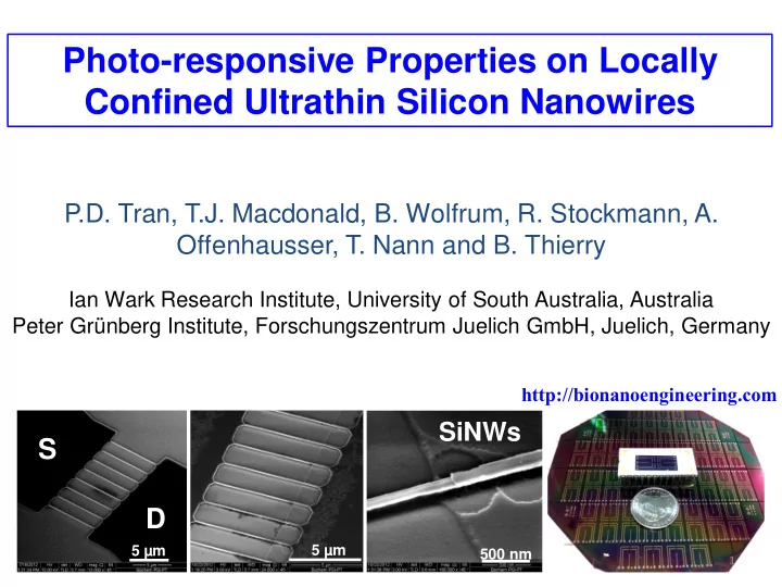
confined ultrathin silicon nanowires
play

Confined Ultrathin Silicon Nanowires P.D. Tran, T.J. Macdonald, B. - PowerPoint PPT Presentation

Photo-responsive Properties on Locally Confined Ultrathin Silicon Nanowires P.D. Tran, T.J. Macdonald, B. Wolfrum, R. Stockmann, A. Offenhausser, T. Nann and B. Thierry Ian Wark Research Institute, University of South Australia, Australia Peter


  1. Photo-responsive Properties on Locally Confined Ultrathin Silicon Nanowires P.D. Tran, T.J. Macdonald, B. Wolfrum, R. Stockmann, A. Offenhausser, T. Nann and B. Thierry Ian Wark Research Institute, University of South Australia, Australia Peter Grünberg Institute, Forschungszentrum Juelich GmbH, Juelich, Germany http://bionanoengineering.com SiNWs S D 5 µm 5 µm 500 nm 1

  2. Why Ultrathin Silicon Nanowire ?  Silicon nanowires (SiNWs) are promising functional building blocks for novel optoelectronic devices 1,2  Down-scaling to ultrathin SiNWs open up opportunities to explore new fundamental properties of one-dimensional materials  high performance nanoscaled devices  The performance of planar SiNWs optoelectronic devices is currently limited by the inherent low fill factor and light reflection  CdTe quantum dots (QDs) are high-efficiency fluorescence materials with tuneable emission wavelength  “light harvesting antenna” for ultrathin SiNWs devices Aim: To fabricate and improve the performance of novel, locally confined ultrathin SiNWs photo-resistors 1. Zhang, A.; Kim, H.; Cheng, J.; Lo, Y .-H. Nano Letters 2010, 10, (6), 2117-2120. 2 2. Garnett, E.; Yang, P. Nano Letters 2010, 10, (3), 1082-1087.

  3. The Fabrication 1. SiNWs Patterning 2. Localized Etching 3. Packaging a nm b c d SiNWs patterning by e-beam lithography S and TMAH etching  Wafer-scaled homogeneity of the Si device layer thickness (~ 40nm) D  Highly-ordered SiNWs (WxL: 200 nm 5 µm x10 µm) with smooth trapezoidal shape 500 nm 3

  4. The Fabrication 1. SiNWs Patterning 2. Localized Etching 3. Packaging 0.95 nm 1.2 nm 1.1 nm Optimization of the TMAH wet a c b etching using isopropanol additive for localized etching 4 3.5 -0.1 nm 3 0.12 nm 0.0 nm Etch rate (nm/s) 35 o C 45 o C Pristine Si 2.5 1.3 nm 1.4 nm 3 nm 2 d e f 1.5 1 0.5 0 65 55 45 35 Temperature ( o C) -0.1 nm 0.0 nm 0.0 nm 55 o C 65 o C Oxidation + HF  A very slow (~0.5 nm/s) and well-controlled TMAH etching rate on Silicon (100) was obtained  Atomic smooth Si surface is maintained after etching (rms roughness ~0.15 nm) 4

  5. The Fabrication 1. SiNWs Patterning 2. Localized Etching 3. Packaging 40 nm e f 20 nm 5 µm 500 nm Ultrathin SiNW 40 nm SiO 2 SiO 2 Si 20 nm Si 200 nm 100 nm Ultrathin SiNWs were fabricated with thickness down to ~20 nm by localized wet-etching with optimized TMAH  Compatible with device integration techniques  Thickness scalable to sub-20 nm 5  Straight forward and easy to implement

  6. The Fabrication 1. SiNWs Patterning 2. Localized Etching 3. Packaging g h j i A novel wafer-scaled top-down process for the fabrication of locally thinned-down silicon nanowires based device has been developed 6

  7. Ultrathin SiNWs Characterizations Ids (µA) a c Vds (V)  High photosensitive, LOD: 0.75 4.2 1.28 1.2 b mW.cm -2  High photoresponsivity, R ~ 10 4 A/W 4.0 Ids (µA) >> 0.7A/W ( commercial silicon PIN 3.8 photodiode) 0.85  Good time response: t = 0.003s 3.6 0.75 0.5 Dark  High mobility photocarriers are 3.4 generated in high quality ultrathin SiNWs -100 0 100 200 300 400 500 600 700 Time (s) 7

  8. Ultrathin SiNWs Characterization 4 24 Dark a c 254 nm ON 20 3 365 nm Ids (µA) Ids (µA) 680 nm 16 2 12 Bias at 2.0 V 8 1 Bias at -2.0 V OFF 4 0 0 ON -4 -1 -8 0 5 10 15 20 -3 -2 -1 0 1 2 3 Vds (V) Time (minute)  Broad light detection spectrum: 254 nm 25 273 K  680 nm 298 K 20 313 K  Thermal stability: 0 o C  70 o C 343 K Ids (µA) 15  Long-term stable measurement: 20 mins 10 5  Highly photo-responsive and stable 0 ultrathin SiNWs b -5 -10 -3 -2 -1 0 1 2 3 8 Vds (V)

  9. Quantum dot – SiNWs hybrids Dark 10 Dark a b 40 365 nm/Bare Si Bare Si 365nm/Si-QD Si/QD 8 680nm/Bare Si 680nm/Si-QD 30 Ids (µA) Ids (µA) 6 20 4 10 2 0 0 0.0 0.2 0.4 0.6 0.8 1.0 -0.5 0.0 0.5 1.0 1.5 2.0 2.5 3.0 3.5 Vds (V) Vds (V)  10 nm CdTe quantum dots nanoparticle were successfully synthesised  ~ 59 ± 10% improvement in photocurrent response of QD-SiNWs measure under 365 nm UV light due the QDs emitting in the visible region.  Initial measurement on solar full spectrum (300  1400 nm; 100 mW/cm 2 ) show ~20 % increasing in photocurrent response  Fast, stable and highly photoresponsive new nanostructures based on quantum dots - SiNWs hydrids have been developed 9

  10. Conclusion and Outlook  A novel and straight-forward top-down fabrication of functional ultrathin SiNWs has been developed  The fabricated ultrathin SiNWs have demonstrated ultrahigh photo-responsivity, high photosensitivity, stability, durability and fast response  QD modified SiNWs have shown an improvement of the photocurrent measured under UV light while preserving their performance in visible light Potential to apply this novel process to fabricate sub-10 nm thin SiNWs Exciting applications for opto-electronics and photovoltaics hydrid systems 10

  11. Acknowledgements - Dr. Dirk Mayer, Dr. Venesa Maybeck, Dr. Stefan Trellenkamp - Forschungszentrum Jülich, Germany - Dr. Xuan Thang Vu - University of Applied Sciences Kaiserslautern, Germany - Dr. Tong Duy Hien - Nanosens Research Co., Netherland - Asso/Prof. Steve Madden - Australian National University, Australia - This work was performed in part at the SA and ACT nodes of the Australian National Fabrication Facility, a company established under the National Collaborative Research Infrastructure Strategy to provide nano and micro- fabrication facilities for Australia’s researchers . Thank for the financial support from: + Australian Technology network – German Academic Exchange Service (DAAD) award + NH&MRC 631939 research project 11

Download Presentation
Download Policy: The content available on the website is offered to you 'AS IS' for your personal information and use only. It cannot be commercialized, licensed, or distributed on other websites without prior consent from the author. To download a presentation, simply click this link. If you encounter any difficulties during the download process, it's possible that the publisher has removed the file from their server.

Recommend


More recommend