
SLIDE 1
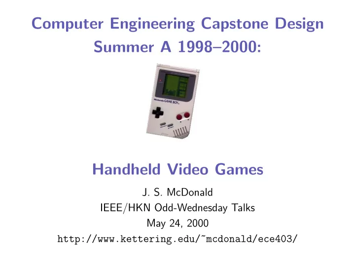
Computer Engineering Capstone Design Summer A 1998–2000: Handheld Video Games
- J. S. McDonald
Computer Engineering Capstone Design Summer A 19982000: Handheld - - PowerPoint PPT Presentation
Computer Engineering Capstone Design Summer A 19982000: Handheld Video Games J. S. McDonald IEEE/HKN Odd-Wednesday Talks May 24, 2000 http://www.kettering.edu/~mcdonald/ece403/ PIC-Pong By Rickard Gun ee; uses a 4-MHz PIC16F84 and a
Slide 1
Slide 2
Slide 3
Slide 4
Slide 5
Slide 6
Slide 7
Tcy0 Tcy1 Tcy2 Tcy3 Tcy4 Tcy5
Fetch 1 Execute 1
Fetch 2 Execute 2
Fetch 3 Execute 3
Fetch 4 Flush
Fetch SUB_1 Execute SUB_1
Slide 8
Mnemonic, Operands Description Cycles 14-Bit Instruction Word Status Bits Affected Notes MSb LSb BYTE-ORIENTED FILE REGISTER OPERATIONS ADDWF ANDWF CLRF CLRW COMF DECF DECFSZ INCF INCFSZ IORWF MOVF MOVWF NOP RLF RRF SUBWF SWAPF XORWF f, d f, d f
f, d f, d f, d f, d f, d f, d f
f, d f, d f, d f, d Add W and f AND W with f Clear f Clear W Complement f Decrement f Decrement f, Skip if 0 Increment f Increment f, Skip if 0 Inclusive OR W with f Move f Move W to f No Operation Rotate Left f through Carry Rotate Right f through Carry Subtract W from f Swap nibbles in f Exclusive OR W with f 1 1 1 1 1 1 1(2) 1 1(2) 1 1 1 1 1 1 1 1 1 00 00 00 00 00 00 00 00 00 00 00 00 00 00 00 00 00 00 0111 0101 0001 0001 1001 0011 1011 1010 1111 0100 1000 0000 0000 1101 1100 0010 1110 0110 dfff dfff lfff 0xxx dfff dfff dfff dfff dfff dfff dfff lfff 0xx0 dfff dfff dfff dfff dfff ffff ffff ffff xxxx ffff ffff ffff ffff ffff ffff ffff ffff 0000 ffff ffff ffff ffff ffff C,DC,Z Z Z Z Z Z Z Z Z C C C,DC,Z Z 1,2 1,2 2 1,2 1,2 1,2,3 1,2 1,2,3 1,2 1,2 1,2 1,2 1,2 1,2 1,2 BIT-ORIENTED FILE REGISTER OPERATIONS BCF BSF BTFSC BTFSS f, b f, b f, b f, b Bit Clear f Bit Set f Bit Test f, Skip if Clear Bit Test f, Skip if Set 1 1 1 (2) 1 (2) 01 01 01 01 00bb 01bb 10bb 11bb bfff bfff bfff- bfff ffff ffff ffff ffff 1,2 1,2 3 3 LITERAL AND CONTROL OPERATIONS ADDLW ANDLW CALL CLRWDT GOTO IORLW MOVLW RETFIE RETLW RETURN SLEEP SUBLW XORLW k k k
k k
k Add literal and W AND literal with W Call subroutine Clear Watchdog Timer Go to address Inclusive OR literal with W Move literal to W Return from interrupt Return with literal in W Return from Subroutine Go into standby mode Subtract W from literal Exclusive OR literal with W 1 1 2 1 2 1 1 2 2 2 1 1 1 11 11 10 00 10 11 11 00 11 00 00 11 11 111x 1001 0kkk 0000 1kkk 1000 00xx 0000 01xx 0000 0000 110x 1010 kkkk kkkk kkkk 0110 kkkk kkkk kkkk 0000 kkkk 0000 0110 kkkk kkkk kkkk kkkk kkkk 0100 kkkk kkkk kkkk 1001 kkkk 1000 0011 kkkk kkkk C,DC,Z Z TO,PD Z TO,PD C,DC,Z Z Note 1: When an I/O register is modified as a function of itself ( e.g., MOVF PORTB, 1), the value used will be that
Slide 9
EPROM Program Memory 13 Data Bus 8
Program Bus Instruction reg Program Counter 8 Le
(13-bit) RAM File Registers Direct Addr 7 RAM Addr (1)
✁9
✂Addr MUX Indirect Addr
✄FSR reg STATUS reg MUX ALU
✄W reg
☎Power-up Timer
✆Oscillator
✝Start-up Timer Power-on Reset W
☎atchdog Timer
✆Instruction Decode & Control Timing
✆Generation OSC1/CLKIN
✝OSC2/CLK
✝OUT MCLR V
✞DD
✟, VSS
✠PORTA PORTB PORTC PORTD PORTE RA4/T0CKI RA5/SS/AN4
✡RB0/INT RB7:RB1 RC0/T1OSO/T1CKI RC1/T1OSI/CCP2 RC2/CCP1 RC3/SCK/SCL RC4/SDI/SDA RC5/SDO RC6/TX/CK RC7/RX/DT RD7/PSP7:RD0/PSP0 RE0/RD/AN5
✡RE1/WR/AN6
✡RE2/CS/AN7
✡8
Reset(2)
✁USART CCP1 CCP2 Synchronous A/D Timer0 Timer1 Timer2 Serial Port RA3/AN3/VREF
☛RA2/AN2 RA1/AN1 RA0/AN0 Parallel Slave Port 8
Slide 10
INDF(1) TMR0 PCL STATUS FSR PORTA PORTB PORTC PORTD(2) PORTE(2) PCLATH INTCON PIR1 PIR2 TMR1L TMR1H
TMR2 T2CON SSPB
✂UF SSPCON CCPR1L CCPR1H
✁CCP1CON RCSTA TXREG RCREG CCPR2L CCPR2H
✁CCP2CON ADRES
✝ADCON0 INDF(1) OPTION
✞PCL STATUS FSR TRISA TRISB
TRISD(2) TRISE(2) PCLATH INTCON PIE1 PIE2 PCON PR2 SSP
✂ADD SSPST
✂AT TXSTA SPBRG
✂ADCON1
✝00h 01h 02h 03h 04h 05h 06h 07h 08h 09h 0Ah 0Bh 0Ch 0Dh 0Eh 0Fh 10h 11h 12h 13h 14h 15h 16h 17h 18h 19h 1Ah 1Bh 1Ch 1Dh 1Eh 1Fh 80h 81h 82h 83h 84h 85h 86h 87h 88h 89h 8Ah 8Bh 8Ch 8Dh 8Eh 8Fh 90h 91h 92h 93h 94h 95h 96h 97h 98h 99h 9Ah 9Bh 9Ch 9Dh 9Eh 9Fh 20h A0h Gener
✟al Purpose Register Gener
✟al Purpose Register 7Fh FFh Bank 0 Bank 1 File Address File Address
Slide 11
Slide 12
VDD VDD MCLR RA0 RA1 RA2 RA3 RA4 RA5 RB0 RB1 RB2 RB3 RB4 RB5 RB6 RB7 OSC1 VSS VSS 11 32 1 2 3 4 5 6 7 33 34 35 36 37 38 39 40 13 12 31
U1 PIC16C64
+5V C2 NMCLR RA0 RA1 RA2 RA3 RA4 RA5 RB0 RB1 RB2 RB3 RB4 RB5 RB6 RB7 RD0 RD1 RD2 RD3 RD4 RD5 RD6 RD7 OS0 OS1 RC2 SCL SDA RC5 TX RX RB +5V R16 5K 470 C16 0.01 LM78L05 U5 IN OUT COM 1 4 2 3 W02M CR1 +9V Battery
J2
1 3 2 DJ005A C18 220 C19 0.1 VCC 2 11 10 12 9 1 3 6
U3
MAX232A +5V C12 0.1 TX RX 14 7 13 8 4 5 V+ T1IN T2IN R1OUT R2OUT C1+ C1- V- T1OUT T2OUT R1IN R2IN C2+ C2- GND 15 C14 0.1 C11 0.1 C15 0.1 1 2 3 4 5 6 7 8 9 J1 16
+
Notes: Unless otherwise specified, resistance values are in ohms, 5% 1/4W. Capacitance values are in microfarads.
0.1 RE0 RE1 RE2 RD0 RD1 RD2 RD3 RD4 RD5 RD6 RD7 RC0 RC1 RC2 RC3 RC4 RC5 RC6 RC7 OSC2 8 9 10 19 20 21 22 27 28 29 30 15 16 17 18 23 24 25 26 14 1 2 3 4 5 6 7 8 R1 4.7K S1 +5V C1 0.1 +5V R4 4.7K C3 20PF OSC1
Provision Only
1 2 3 4 5 6 RA0 RA1 RA2 RA3 RA4 RA5 R2 S2 +5V R3 4.7K A0 A1 A2 SCL WP 1 2 3 6 7
U4
SDA +5V 5
24LC01B
VDD VSS C10 0.1 +5V +5V X1 CR2 1N914
+
C17 220 VDD MCLR RA0 RA1 RA2 RA3 RA4 RA5 RB0 RB1 RB2 RB3 RB4 RB5 RB6 RB7 VSS VSS 20 1 2 3 4 5 6 7 21 22 23 24 25 26 27 28 8 19
U2 PIC16C73
+5V C8 NMCLR RA0 RA1 RA2 RA3 RA4 RA5 RB0 RB1 RB2 RB3 RB4 RB5 RB6 RB7 OSC1 OSC2 0.1 OSC1 OSC2 RC0 RC1 RC2 RC3 RC4 RC5 RC6 RC7 9 10 11 12 13 14 15 16 17 18 OSO OSI RC2 SCL SDA RC5 TX RX RE0 RE1 RE2 RE +5V R5 10K R6 330 J3 +5V 1 2 3 4 5 6 7 8 9 10 11 12 13 14 RA1 RA2 RA3 FOR LCD DSPLY R7 4.7K S3 +5V C9 0.1 C13 0.1 R14 10 +5V R15 470 GRN POWER D1 J8 Y1 TBD C4 20PF C5 20PF
Not Populated
OUT TXCO RC 1 2 3 4 5 6 7 8 OSO OSI RC2 SCL SDA RC5 TX RX (RC0) (RC1) (RC3) (RC4) (RC6) (RC7) RD 1 2 3 4 5 6 7 8 RD0 RD1 RD2 RD3 RD4 RD5 RD6 RD7 J4 1 2 3 4 5 6 7 8 9 KEYBOARD 9 PIN HEADER RB0 RB1 RB2 RB3 RN3 RB4 RN3 RB5 RN3 RB6 RN3 RB7 RN1 RB0 RN1 RB1 RN1 RB2 RN1 RB3 RN2 RB4 RN2 RB5 RN2 RB6 RN2 RB7 D2 D3 D4 D5 D6 D7 D8 D9 J7 J6 OSC2
Provision Only, Not Populated
Y3 TBD C6 20pF C7 20pF +5V R10 10 R11 10 R12 820 R8 10 R9 10 R13 820 +5V +5V RA Y2 J5
8
Breadboard R19 470 R17 470 R18 470 4 3 RN3 4 4 4 3 3
Slide 13
Slide 14
SRAM 8Kx8 bits LCD 128x128 T6963C
FS RESET C/D CE RD WR D7-D0
Bias Circuit
VEE VDD VSS
Toshiba Controller
Slide 15
Slide 16
Optimal for lightweight, portable products.
No software development required, quick time to market
Authentic, natural sounding voice and music reproduction
Ideal for battery-powered applications.
Power failure protection
Meets consumer market demands
Voice record and playback system on a single chip 6 seconds to 8 minutes record and playback durations Industry-leading sound quality Fully integrated system functions: AGC, mic preamp, speaker drivers, filters, oscillator, memory Low voltage operation Message management Flexible architecture Battery-less message storage
Slide 17
9 VSS 10 RESET 20 IRQ 19 PA7 11 PA6 12 PA5 13 PA4 14 PA3 15 PA2 16 PA1 17 PA0 18 PB5 3 PB4 4 PB3 5 PB2 6 PB1 7 PB0 8 OSC1 1 OSC2 2 U1 M68HC705J1A VCC A9 10 A8 9 A7 8 A6 7 A5 6 A4 5 A3 4 A2 3 A1 2 PD 24 P/R 27 EOM 25 VCCD 28 VCCA 16 SP+ 14 SP- 15 MIC REF 18 MIC 17 VSSA 13 VSSD 12 AUX IN 11 ANA IN 20 ANA OUT 21 AGC 19 XCLK 26 OVF 22 CE 23 A0 1 U2 ISD2545 VCC
✁LS1 SPEAKER J1 PHONEJACK P2 PHONEPLUG GND GND GND R1 470K C1 4.7uF R4 10 GND VCC
Slide 18
Slide 19
Slide 20
Parallel Cable Power Supply Cable Emulator Pod Processor Module with Ca
✠ble Logic Probe Connector Device Adapter
Slide 21