
SLIDE 1
- M. Wuttig and N. Yamada, Nature Mater. 6, 824 (2007).
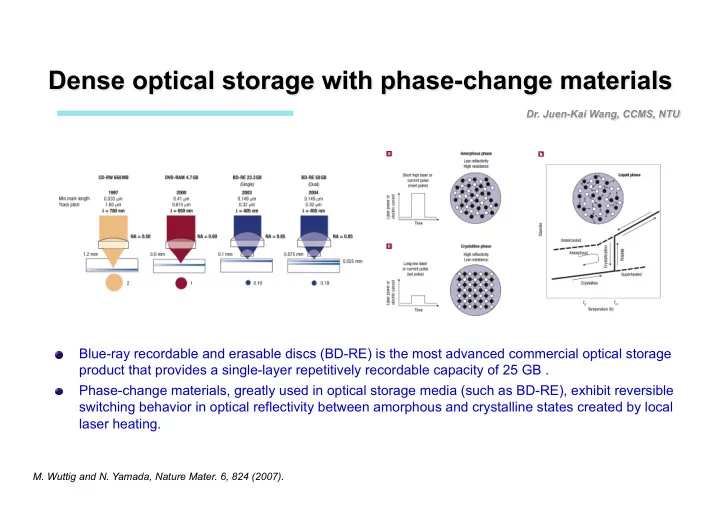
- Blue-ray recordable and erasable discs (BD-RE) is the most advanced commercial optical storage
product that provides a single-layer repetitively recordable capacity of 25 GB .
- Phase-change materials, greatly used in optical storage media (such as BD-RE), exhibit reversible