Ascatron Offer Ascatron is an independent producer of SiC material - - PDF document

ascatron offer
SMART_READER_LITE
LIVE PREVIEW

Ascatron Offer Ascatron is an independent producer of SiC material - - PDF document

SILICON CARBIDE EPI & DEVICE Ascatron Offer Ascatron is an independent producer of SiC material and devices offering the complete fabrication from epitaxy to diced wafers. Ascatron provides unique technology on 3DSiC epitaxial structures


slide-1
SLIDE 1

SILICON CARBIDE EPI & DEVICE

Ascatron 2013-09-27 1(4)

Ascatron Offer

Ascatron is an independent producer of SiC material and devices offering the complete fabrication from epitaxy to diced wafers. Ascatron provides unique technology on 3DSiC epitaxial structures enabling high quality material and advanced device concepts. Ascatron offer a number of device designs for power diodes and switches which are optimised to meet the device specifications. The focus is on fast delivery of wafers in small series for development and market verification. Ascatron scale-up the SiC epitaxial material production in accordance with the customer’s needs.

SiC Material & Device Solutions

Custom Specific Design

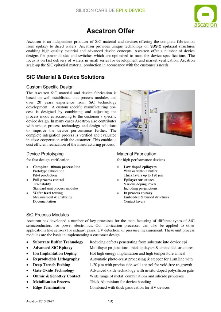
The Ascatron SiC material and device fabrication is based on well established unit process modules and

  • ver 20 years experience from SiC technology
  • development. A custom specific manufacturing pro-

cess is designed by combining and adjusting the process modules according to the customer’s specific device design. In many cases Ascatron also contributes with unique process technology and design solutions to improve the device performance further. The complete integration process is verified and evaluated in close cooperation with the customer. This enables a cost efficient realization of the manufacturing process.

Device Prototyping

for fast design verification

 Complete 100mm process line Prototype fabrication Pilot production  Full process control Traceability Standard unit process modules  Wafer level testing Measurement & analyzing Documentation

Material Fabrication

for high performance devices

 Low doped epilayers With or without buffer Thick layers up to 180 µm  Epilayer structures Various doping levels Including pn-junctions  In process epitaxy Embedded & buried structures Contact layers

SiC Process Modules

Ascatron has developed a number of key processes for the manufacturing of different types of SiC semiconductors for power electronics. Our fabrication processes can also be applied to other applications like sensors for exhaust gases, UV detection, or pressure measurement. These unit process modules are the basis in implementing a customer design.  Substrate Buffer Technology Reducing defects penetrating from substrate into device epi  Advanced SiC Epitaxy Multilayer pn-junctions, thick epilayers & embedded structures  Ion Implantation Doping Hot high energy implantation and high temperature anneal  Reproducible Lithography Automatic photo-resist processing & stepper for 1µm line with  Deep Trench Etching 1-20 µm with precise side-wall control for void-free re-growth  Gate Oxide Technology Advanced oxide technology with in-situ-doped polysilicon gate  Ohmic & Schottky Contact Wide range of metal combinations and silicide processes  Metallisation Process Thick Aluminium for device bonding  Edge Termination Combined with thick passivation for HV devices

slide-2
SLIDE 2

SILICON CARBIDE EPI & DEVICE

Ascatron 2013-09-27 2(4)

Fabrication Resources

Ascatron SiC epi and device manufacturing is located at the Electrum Laboratory outside Stockholm. The clean-room has a total area of 1300 m2 and provides the access to all equipment needed for processing of 100 mm diameter SiC wafers. The SiC process line has a capacity of 1000 wafers per year. Process Type Parameters Tools Cap

Epitaxy Hot-wall CVD n/p 4H-, 6H, 3C-SiC n-doping 1014-1019 cm-3 p-doping 1014-1020 cm-3 Thickness up to 180 µm 2 Aixtron VP508GFR S Doping Ion Implanter 40-330keV - Al, B, N, P RT & 600 ºC Danfysik 1090* S Furnace Processes Thermal Oxidations Wet/Dry/N2O (900-1250ºC) Thermco 5200 B LPCVD LTO, TEOS, Polysilicon Bruce Furnace B Annealing 1400-1800 ºC in Ar Centrotherm Activator 150 B RTP Mattson 100 RTP S Plasma Deposition PECVD SiO2, Si3N4 Oxford Plasmalab 80 Applied Materials P5000 S S Plasma Etching RIE Oxford Plasmalab 80 Oxford Plasmalab 100 Applied Materials P5000 S S S ICP STS ICP DRIE Oxford ICP380 S S Microwave plasma ash O2 TePla300 B Wet Etching Wet cleaning process Acid and solvent based B Metallisation Plasma sputter Au, Ni, Al, Ag, TiW KDF 844NT, MRC 643 B Ion-beam sputter Au, Ni, Al, Ti Commonwealth IBS B Evaporation Au PAK600 B Lithography Contact Alignment Accuracy ~1μm Minimum Features ~1.5 μm Karl Suss MA8 S Stepper Alignment Accur. ~ 0.3 μm Minimum Features ~ 1μm ALS 2035 G-line S Lift-off B Metrology SEM Zeiss Ultra 55, Hitachi S-3400N S S Ellipsometer Horiba Uvisel ER SENTECH instrum. S S Surface Profiler Tencor-P10, Dektak3ST S S AFM Veeco Dimension 3100 S Sheet Resistance 4-point probe Four Dimension 280 S Inspection Microscope Nikon, Olympus, Leitz S Testing Automated Probing Karl Suss PA 150 Electroglass S B Dicing High Speed Saw Disco DFD640 S

Capacity of respective tool is marked as single wafer (S) and batch processing (B). Equipment excluding epitaxy, RTP and LPCVD also compatible with 150 mm substrates. * Performed at Ion Technology Center, Ångström Laboratoty in Uppsala

slide-3
SLIDE 3

SILICON CARBIDE EPI & DEVICE

Ascatron 2013-09-27 3(4)

SiC Device Technologies

Ascatron offer a number of power device technologies as the basis for the custom specific device

  • design. The process can be optimized to meet the specific requirements, e.g. packaging compatible

metallisation.  Schottky diode For material evaluation  JBS diode Both implanted and epitaxial 3DSiC concepts  HV-PiN diode Epitaxial anode and pn-junction grown in one run  Vertical DMOSFET Advanced gate oxide technology using deposited oxides  Epitaxial buried grid JFET Based on embedded epitaxial technology

EPS Diode

The Ascatron Epitaxial PN Schottky diode (EPS) technology is based on a proprietary concept utilizing a buried grid as junction barrier. With an additional epitaxy layer we design a thicker second drift region above the p+ emitter grid. The important function of the buried grid is the reduction of the leakage current due to efficient reduction of the surface field under the Schottky

  • contact. This gives 3 orders of magnitude lower

leakage current compared to the conventional JBS surface grid design, thus allowing increas- ing the max operation temperature from 175°C up to 250°C. The concept also makes it possible to replace the implanted emitter with an epitaxial grown and etched grid using Ascatron 3DSiC technology. The high crystalline quality, free from implan- tation damage results in better injection effici-

  • ency. This improves the surge current capability

and high temperature properties even further. Ascatron offer customized fabrication of 1200V EPS diodes. We are currently developing the device technology for 1700V and 3,3 kV devices.

3DSiC Technology

A basic problem in the fabrication of SiC devices resides in the conventional process for doping with ion implantation. This introduces damages that cannot be annealed. Diffusion is very slow in the wide band gap material and prevents healing of the defects. Also the activation of the doping ions is

  • inhibited. This limits the real performance of SiC devices regarding temperature range, current density

and high voltage performance. Ascatron’s solution is to replace ion implantation doping with epitaxial growth in etched 3 dim- ensional structures – 3DSiC. This results in extremely good material quality, and thus very stable high temperature performance. The 3DSiC technology also enables new advanced design concepts for active devices with high doping and small lateral dimensions resulting in lower losses and thus less self-heating. The potential of the 3DSiC technology has been successfully demonstrated in an all epitaxial buried grid normally-off JFET switch. The 3DSiC technology can also be used to make a very efficient buffer layer between substrate and epitaxial device layer to reduce defects. This is designed to sustain high blocking voltages and handling high current densities. With our 3DSiC technology we can thus keep the stacking faults in the substrate, where they do no harm, and prevent them from penetrating into the drift layer. Patent pending design EP2154726 Reduced surface field P+ N- N+ Schottky contact

Figure 1. EPS diode design showing the simulated electri- cal field at blocking. The buried emitter grid reduces the leakage current, allowing operating temperature of 250°C.

slide-4
SLIDE 4

SILICON CARBIDE EPI & DEVICE

Ascatron 2013-09-27 4(4)

Figure 2. Ascatron 3DSiC technology replaces ion implantation with epitaxial grown doping structures. This enables the design of high performance SiC power devices with stable high temperature operation. The superior material quality and design flexibility is also advantageous for realisation of high voltage devices with high current densities.

Company

Ascatron started its operation in 2011 as a spin-out from the Swedish research institute Acreo. The team of 10 persons have a long experience in the development of SiC epitaxial material and process technology to realise high performance SiC devices. The development of the SiC technology was started 1993 at Acreo. In a joint project with ABB a 4.5 KV PiN- diode was demonstrated in 1999. A SiC MESFET was developed in 2002 and spun-out to AMDS in 2002. Acreo started to offer SiC epitaxy as a service, specialising on multi-layer structures and re-growth on non-planar surfaces. Several SiC device concepts were developed and a collaboration with DENSO Corporation, Japan resulted in the realisation of a normally-off SiC JFET with ratings of 1.2 kV and 50 A. Acreo also had a long cooperation with HOYA Corporation, Japan, on the development of the 3C-SiC process technology for power MOSFET demonstrating very high channel mobility and blocking up to 1000V. Ascatron is Partner Company of the SiC Power Center in Sweden and participates in several EU research projects.

Contact Information

Ascatron AB

Isafjordsgatan 22 Electrum 207 SE-16440 Kista - Stockholm Sweden VAT nr: SE556860369901 www.ascatron.com info@ascatron.com Fax: +46 8 750 5430

Director Technology & Sales

Adolf Schöner Tel: +46 70 792 7809 adolf.schoner@ascatron.com

Managing Director

Christian Vieider Tel: +46 70 2171 654 christian.vieider@ascatron.com

Chairman

Bo Hammarlund Tel: +46 70 741 2622 bo.hammarlund@ascatron.com

N

Etch

N P N

Planarize 3D SiC Epi

Figur 3. Ascatron is Partner Company of the SiC Power Center in Sweden. The organisation with 14 member companies (e.g. Alstom, ABB, Bombardier, Volvo, Kolmorgen) and research

  • rganisations has the objective to speed up the

implementation of SiC power devices. The center is organising the yearly workshop on SiC power electronics applications ISiCPEAW.