
SLIDE 1
Architecture
Calcolatori Elettronici e Sistemi Operativi
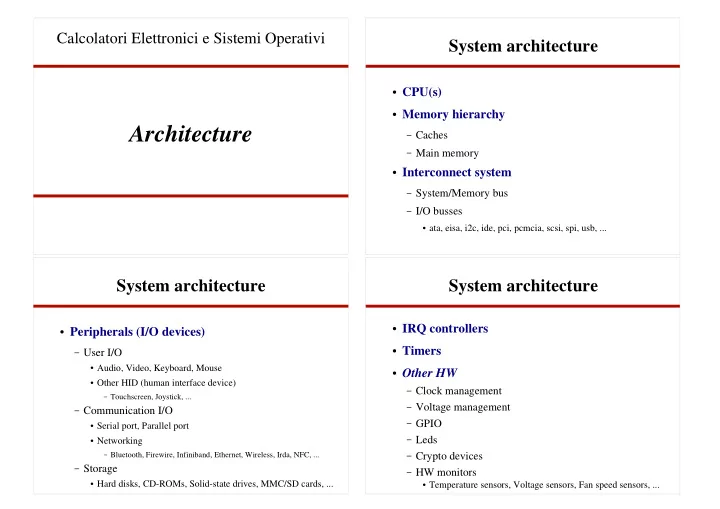
System architecture
CPU(s) Memory hierarchy
– Caches – Main memory
Interconnect system
– System/Memory bus – I/O busses
ata, eisa, i2c, ide, pci, pcmcia, scsi, spi, usb, ...
System architecture
Peripherals (I/O devices)
– User I/O
Audio, Video, Keyboard, Mouse Other HID (human interface device)
– Touchscreen, Joystick, ...
– Communication I/O
Serial port, Parallel port Networking
– Bluetooth, Firewire, Infiniband, Ethernet, Wireless, Irda, NFC, ...
– Storage
Hard disks, CD-ROMs, Solid-state drives, MMC/SD cards, ...
System architecture
IRQ controllers Timers Other HW
– Clock management – Voltage management – GPIO – Leds – Crypto devices – HW monitors
Temperature sensors, Voltage sensors, Fan speed sensors, ...