
SLIDE 1
| 1
SCALING ROADMAP
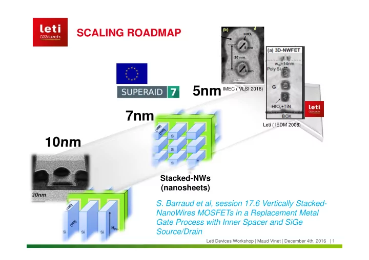
10nm 7nm 5nm
Stacked-NWs (nanosheets)
IMEC ( VLSI 2016) Leti Devices Workshop | Maud Vinet | December 4th, 2016
- S. Barraud et al, session 17.6 Vertically Stacked-
NanoWires MOSFETs in a Replacement Metal Gate Process with Inner Spacer and SiGe Source/Drain
Leti ( IEDM 2008)