
SLIDE 1
2/13/2014 1
Physical Attacks and Tamper Resistance
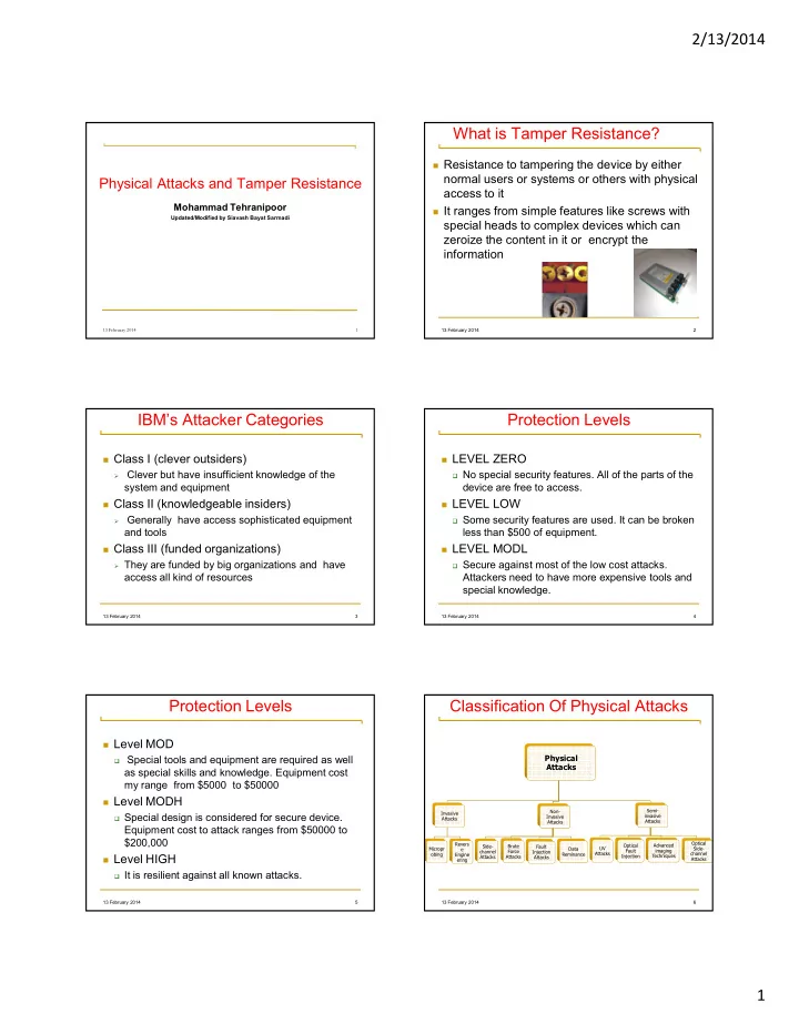
- What is Tamper Resistance?
Resistance to tampering the device by either
normal users or systems or others with physical access to it
It ranges from simple features like screws with
special heads to complex devices which can zeroize the content in it or encrypt the information
13 February 2014 2
IBM’s Attacker Categories
Class I (clever outsiders)
Clever but have insufficient knowledge of the
system and equipment
Class II (knowledgeable insiders)
Generally have access sophisticated equipment
and tools
Class III (funded organizations)
They are funded by big organizations and have
access all kind of resources
13 February 2014 3
Protection Levels
LEVEL ZERO
No special security features. All of the parts of the
device are free to access.
LEVEL LOW
Some security features are used. It can be broken
less than $500 of equipment.
LEVEL MODL
Secure against most of the low cost attacks.
Attackers need to have more expensive tools and special knowledge.
13 February 2014 4
Protection Levels
Level MOD
Special tools and equipment are required as well
as special skills and knowledge. Equipment cost my range from $5000 to $50000
Level MODH
Special design is considered for secure device.
Equipment cost to attack ranges from $50000 to $200,000
Level HIGH
It is resilient against all known attacks.
13 February 2014 5
Classification Of Physical Attacks
- !"
- #
- $%
#
- 13 February 2014
6