1
play

1 Trace Cache Summary of Reducing Cache Hit Time Trace: a dynamic - PDF document

Improving Cache Performance 1. Reducing miss rates 3. Reducing miss penalty or miss rates via parallelism Larger block size Lecture 18: Reducing Cache Hit Non-blocking caches larger cache size Time and Main Memory Design


  1. Improving Cache Performance 1. Reducing miss rates 3. Reducing miss penalty or miss rates via parallelism Larger block size Lecture 18: Reducing Cache Hit � Non-blocking caches larger cache size � Time and Main Memory Design Hardware prefetching higher associativity � Compiler prefetching victim caches � way prediction and � 4. Reducing cache hit time Virtual Cache, pipelined cache, cache Pseudoassociativity � Small and simple summary, main memory technology compiler optimization � caches 2. Reducing miss penalty � Avoiding address Multilevel caches translation � critical word first � Pipelined cache access � read miss first � Trace caches � merging write buffers � 1 2 Adapted from UC Berkeley CS252 S01 Fast Cache Hits by Avoiding 
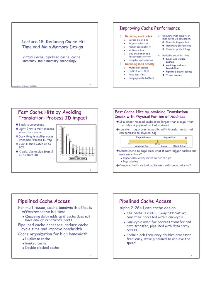
Fast Cache Hits by Avoiding Translation: Index with Physical Portion of Address Translation: Process ID impact If a direct mapped cache is no larger than a page, then Black is uniprocess the index is physical part of address Light Gray is multiprocess can start tag access in parallel with translation so that when flush cache can compare to physical tag Dark Gray is multiprocess Page Address 0 Page Offset when use Process ID tag Y axis: Miss Rates up to 12 31 11 0 Address Tag Index Block Offset 20% Limits cache to page size: what if want bigger caches and X axis: Cache size from 2 uses same trick? KB to 1024 KB � Higher associativity moves barrier to right � Page coloring Compared with virtual cache used with page coloring? 3 4 Pipelined Cache Access Pipelined Cache Access For multi-issue, cache bandwidth affects Alpha 21264 Data cache design effective cache hit time � The cache is 64KB, 2-way associative; � Queueing delay adds up if cache does not cannot be accessed within one-cycle have enough read/write ports � One-cycle used for address transfer and Pipelined cache accesses: reduce cache data transfer, pipelined with data array cycle time and improve bandwidth access Cache organization for high bandwidth � Cache clock frequency doubles processor � Duplicate cache frequency; wave pipelined to achieve the speed � Banked cache � Double clocked cache 5 6 1

  2. Trace Cache Summary of Reducing Cache Hit Time Trace: a dynamic sequence of Small and simple caches: used for L1 instructions including taken branches inst/data cache � Most L1 caches today are small but set- Traces are dynamically constructed by associative and pipelined (emphasizing processor hardware and frequently throughput?) used traces are stored into trace � Used with large L2 cache or L2/L3 caches cache Avoiding address translation during indexing cache Example: Intel P4 processor, storing � Avoid additional delay for TLB access about 12K mops 7 8 What is the Impact of What Cache Optimization Summary We’ve Learned About Caches? Technique MP MR HT Complexity 1960-1985: Speed Multilevel cache + 2 = ƒ(no. operations) 1000 CPU Critical work first + 2 1990 penalty miss Read first + 1 � Pipelined Merging write buffer + 1 100 Execution & Victim caches + + 2 Fast Clock Rate Larger block - + 0 � Out-of-Order Larger cache + - 1 miss rate 10 execution Higher associativity + - 1 � Superscalar DRAM Way prediction + 2 Instruction Issue 1 Pseudoassociative + 2 1998: Speed = 1980 1981 1982 1983 1984 1985 1986 1987 1988 1989 1990 1991 1992 1993 1994 1995 1996 1997 1998 1999 2000 Compiler techniques + 0 ƒ(non-cached memory accesses) What does this mean for � Compilers? Operating Systems? Algorithms? Data Structures? 9 10 Main Memory Background Cache Optimization Summary Performance of Main Memory: � Latency: Cache Miss Penalty Technique MP MR HT Complexity � Access Time : time between request and word arrives Nonblocking caches + 3 � Cycle Time : time between requests penalty Hardware prefetching + 2/3 miss � Bandwidth: I/O & Large Block Miss Penalty (L2) Software prefetching + + 3 Main Memory is DRAM : Dynamic Random Access Memory Small and simple cache - + 0 � Dynamic since needs to be refreshed periodically (8 ms, 1% time) Avoiding address translation + 2 hit time � Addresses divided into 2 halves (Memory as a 2D matrix): Pipeline cache access + 1 � RAS or Row Access Strobe Trace cache + 3 � CAS or Column Access Strobe Cache uses SRAM : Static Random Access Memory � No refresh (6 transistors/bit vs. 1 transistor Size : DRAM/SRAM ­ 4-8 , even more today Cost/Cycle time : SRAM/DRAM ­ 8-16 11 12 2

  3. Key DRAM Timing Parameters DRAM Internal Organization Row access time: the time to move data from DRAM core to the row buffer (may add time to transfer row command) � Quoted as the speed of a DRAM when buy � Row access time for fast DRAM is 20-30ns Column access time: the time to select a block of data in the row buffer and transfer it to the processor � Typically 20 ns Cycle time: between two row accesses to the same bank Data transfer time: the time to transfer a block (usually cache block); determined by bandwidth � PC100 bus: 8-byte wide, 100MHz, 800MB/s bandwidth, 80ns to transfer a 64-byte block � Direct Rambus, 2-channel: 2-byte wide, 400MHz DDR, 3.2GB/s bandwidth, 20ns to transfer a 64-byte block Additional time for memory controller and data path inside processor Square root of bits per RAS/CAS 13 14 DRAM History Independent Memory Banks DRAMs: capacity +60%/yr, cost –30%/yr � 2.5X cells/area, 1.5X die size in ­ 3 years How many banks? ‘98 DRAM fab line costs $2B number banks ≤ number clocks to access word in bank � DRAM only: density, leakage v. speed � For sequential accesses, otherwise may Rely on increasing no. of computers & memory per return to original bank before it has next computer (60% market) word ready � SIMM or DIMM is replaceable unit � Increasing DRAM => fewer chips => harder => computers use any generation DRAM to have banks Commodity, second source industry => high volume, low profit, conservative � Exception: Direct Rambus, 32 banks per � Little organization innovation in 20 years chip, 32 x N banks for N chips Order of importance: 1) Cost/bit 2) Capacity � First RAMBUS: 10X BW, +30% cost => little impact 15 16 Fast Memory Systems: DRAM specific Multiple CAS accesses: several names (page mode) � Extended Data Out (EDO) : 30% faster in page mode New DRAMs to address gap; what will they cost, will they survive? � RAMBUS : startup company; reinvent DRAM interface � Each Chip a module vs. slice of memory � Short bus between CPU and chips � Does own refresh � Variable amount of data returned � 1 byte / 2 ns (500 MB/s per channel) � 20% increase in DRAM area � Direct Rambus: 2 byte / 1.25 ns (800 MB/s per channel) � Synchronous DRAM : 2 banks on chip, a clock signal to DRAM, transfer synchronous to system clock (66 - 150 MHz) � DDR Memory: SDRAM + Double Data Rate, PC2100 means 133MHz times 8 bytes times 2 � Which will win, Direct Rambus or DDR? 17 3

Download Presentation
Download Policy: The content available on the website is offered to you 'AS IS' for your personal information and use only. It cannot be commercialized, licensed, or distributed on other websites without prior consent from the author. To download a presentation, simply click this link. If you encounter any difficulties during the download process, it's possible that the publisher has removed the file from their server.

Recommend


More recommend