vgb vt o vsb vdb log companding advanced nut ut ut i d i
play

! VGB VT O VSB VDB Log-Companding Advanced nUt Ut Ut I D = I - PowerPoint PPT Presentation

ISCAS Monday 29th May 2000 VLSI CMOS Low-Voltage Log-Companding Filters Francisco Serra-Graells Paco.Serra@cnm.es Abstract Introduction Principle of Operation and CMOS Generalization Basic Building Blocks Design Methodology


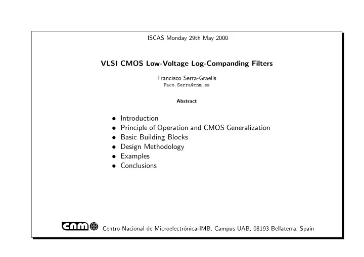
  1. ISCAS Monday 29th May 2000 VLSI CMOS Low-Voltage Log-Companding Filters Francisco Serra-Graells Paco.Serra@cnm.es Abstract • Introduction • Principle of Operation and CMOS Generalization • Basic Building Blocks • Design Methodology • Examples • Conclusions Centro Nacional de Microelectr´ onica-IMB, Campus UAB, 08193 Bellaterra, Spain
  2. Introduction 1 ◮ Instantaneous Companding Processing ◮ Log-Companding law: y = F ( x ) = ex Externally�Linear�Signal�Processing ◮ Previous work mainly in bipolar [1] vs MOS: • Asymmetric I / V curves y in x in Non-linear x out y out Reduced ex current dynamic range -1 Signal�Processing F • F DR y DR DR DR y < • Poor output conductance x y Compression Expansion • Physical mismatching y ≡ Current x ≡ Voltage • Flicker noise ◮ Few CMOS realizations [2] [3] [4] [5] High-Frequency & Low-Voltage Applications ◮ New Proposal ◮ EKV model [6] in weak inversion: VS,DB > VGB − VT O Very�Low-Voltage�Applications n ! VGB − VT O − VSB − VDB Log-Companding Advanced nUt Ut Ut I D = I S e − e e Theory MOSFET�Modeling New�Analog in�Subthreshold Circuit�Techniques D G S B I S = 2 nβU 2 t y=F(x) Francisco Serra-Graells VLSI CMOS Low-Voltage Log-Companding Filters ISCAS 2000/05/29

  3. Principle of Operation 2 ◮ Basic Integrator: d y out = y in . ◮ CMOS Translinear Loops? d t τ ◮ Chain Rule as proposed by [7]: d y out = d y out d x out d x cap d x cap I Di = y out I Dj d t d x out d x cap d t d t M i V GBi CW M j ◮ Product of currents as defined by [8]: V GBj CCW y out C d x cap = C y tun . CW = y tun y in V SBi | {z d t } τ V SBj X X ◮ Multipliers � the Translinear Principle [9]: ( V GB − V SB ) i = ( V GB − V SB ) j y out y cap = y tun y in CCW CW Francisco Serra-Graells VLSI CMOS Low-Voltage Log-Companding Filters ISCAS 2000/05/29

  4. CMOS Generalization 3 ◮ Cancellation of signal dependent terms: X X I Dj n i U t ln I Di + V T Oi + ( n i − 1) V SBi } = n j U t ln + V T Oj + ( n j − 1) V SBj | {z | {z } I Si I Sj CCW CW X X + (1 − 1 I Dj V T Oj + (1 − 1 U t ln I Di + V T Oi ) V GBi = U t ln + ) V GBj I Si n i n i I Sj n j n j | {z } | {z } CCW CW ◮ Gate/Source Driven (G/SD) matched pairs ◮ No GD/SD mixing! GD SD I D 1 I D 2 V 1 M1 M2 NMOS I D 3 I D 4 M3 M4 V 3 V 2 PMOS V 4 ! n 3 ! n 4 ID 1 ID 3 = ID 2 ID 4 IS IS IS IS Francisco Serra-Graells VLSI CMOS Low-Voltage Log-Companding Filters ISCAS 2000/05/29

  5. Basic Building Blocks 4 ◮ Rewriting the product for systematic synthesis: ◮ State-Space matrix description: 8 > < C d x out d I = y tun e xin − xout d t = AI + BIin > d t : Iout = CI + DIin g mAij V j ◮ Proposed CMOS Log-Companding functions: V i 8 > > VT O + nVref > > V > − nUt GD < nUt I capi ISe e I = F ( V ) = > C i > Vref − VT O > > − V > SD : nUt Ut ISe e 8 > X Vj − Vi X Vinj − Vi > N M > > > nUt nUt > + I tunAij e I tunBij e GD > < X X N M d I i d V i j =1 j =1 d t = A ij I j + B ij I inj ⇒ C i d t = > > X Vi − Vj X Vi − Vinj > N M > j =1 j =1 > > Ut Ut − I tunAij e − SD I tunBij e > : j =1 j =1 Francisco Serra-Graells VLSI CMOS Low-Voltage Log-Companding Filters ISCAS 2000/05/29

  6. ◮ Low-Voltage Saturated CMOS cells: Francisco Serra-Graells Basic Building Blocks GD SD I tunAij ( Bi ) nU t C i A ij ( B i ) U t C i A ij ( B i ) I in I in + - + - I bias ORA ORA I bias Compressor V in V ref V ref V in VLSI CMOS Low-Voltage Log-Companding Filters I tunAij(Bi) I tunAij(Bi) V j(in) A ij ( B i ) > 0 V i V j(in) V i VF C i C i j I tunAij(Bi) j j I tunAij(Bi) j V j(in) V i A ij ( B i ) < 0 V j(in) V i VF C i C i V i V i A ii I tunAii C i I tunAii C i j j C j I bias j C j I bias j ORA ORA + - I out + - Expander I out V ref V out V ref V out ISCAS 2000/05/29 5

  7. Basic Building Blocks 6 ◮ Low-Voltage Non-Saturated CMOS cells: ◮ Same Log-Companding F as Saturated SD case, but for A and B : 0 1 Vi − Vj − Vj − Vi Vi X X X N N N B C d Vi Ut Ut Ut Ut @ e A d t = − ItunAije + · · · ≡ − e − ItunAij + . . . Ci ItunAije j =1 j =1 j =1 | {z } j � = i ◮ Signal Boundaries: | Aii | UtCi Ituni 2 I tuni I/I bias 1 1 Aij ( Bi ) > 0 V k S Aik CI 0 Aik < 0 V j V i VF S Aij 5 99% C i I DCi V in S Bi ¢ V/U t 3 90% � � � � 75% � Aij ( Bi ) � � � SAij ( Bi ) 0 50% � � Aii -1 P N Time j =1 Aij + Bi IDCi Ituni | Aii | Francisco Serra-Graells VLSI CMOS Low-Voltage Log-Companding Filters ISCAS 2000/05/29

  8. Basic Building Blocks 7 ◮ Low-Voltage Auxiliary Circuitry: GD SD I in I out X Y Compressor CI CI I in I bias V in V out I in I bias I bias I bias M4 M5 M6 I in I out V ref V in Y V in VF W W V in V out M1 M2 M3 V ref + V out I in X (a) (b) Expander I out j j C I bias I out j j C I bias j j I bias V out V ref I bias V ref V out ◮ Comparison: • Saturated GD � area saving • Saturated SD � technology independence & relaxed matching • Non-Saturated SD � idem Saturated SD & low DC errors Francisco Serra-Graells VLSI CMOS Low-Voltage Log-Companding Filters ISCAS 2000/05/29

  9. Design Methodology 8 ◮ Matrix Procedure A 0 , B 0 and C 0 ( D 0 ≡ 0 ): ◮ Circuit reductions: GD SD 1 Normalize C 0 to share comp/expanders, and Compressor-Expander Yout ( DC ) ≡ Y ( DC ) : I in I in I max I max I bias C 0 M − 1 . - + + - ORA ORA ORA = I ORA + - + - norm I out I out V in 1 j C j j j j 1 C j 1 1 1 V out V in V out 1/ K 1/ K 2 Achieve Y ( DC ) ≡ Yin ( DC ) keeping previous C 1 : I tunAij I tunAij A(B) A ik 1 1 V i A ik A ij C 1 = MopC 1 1 1 A ij V i VF V k V j C i V j C i V k 1 order = − MopA − 1 ¯ B 1¯ 1 inputs 1 I tuni 3 If � ∃ Mop , then use an extra dummy input: 1 1 inputs + ¯ 0 order = A 1¯ ¯ 1 order + B 1¯ V k Bdummy S Aik C I h i V j V i VF B 1 | ¯ S Aij B 2 = Bdummy C i I DCi V in S Bi Francisco Serra-Graells VLSI CMOS Low-Voltage Log-Companding Filters ISCAS 2000/05/29

  10. Design Methodology 9 ◮ Synthesis example: SD Saturated 2nd-Order Low-Pass I max I out 2 I tuno ³ 2 3 2 3 V out = V 1 6 7 6 7 − 2 ζwo − wo 0 ← 6 7 6 7 I in I tuno / 2 ³ I tuno / 2 ³ A = 4 5 B = 4 5 I max - + 0 − wo wo ORA 2 I tuno ³ � � � � V in VF VF V 2 C = 1 0 D = 0 C 2 C 1 I out 2 I tuno ³ 2 3 2 3 6 − 2 ζwo 2 ζwo 7 6 0 7 6 7 6 7 Anew = Bnew = 4 5 4 5 − wo wo V out = V 1 0 2 ζ 2 ζ I in I tuno / 2 ³ I max � � � � + - ORA Cnew = 1 0 Dnew = 0 2 I tuno ³ V in VF VF V 2 C 2 C 1 Francisco Serra-Graells VLSI CMOS Low-Voltage Log-Companding Filters ISCAS 2000/05/29

  11. Design Examples 10 20 ◮ Common specs: 0 • Audio Applications (e.g. Hearing Aids) Current�Gain�[dB] • VDDmin = 1 . 0 V -20 • ( VT ON + | VT OP | ) max = 1 . 25 V -40 • IF ull − Scale = 4 µ A pp • T HD < 1% at 90% Full-Scale -60 • DR = 60dB to 70dB • 10pF < C < 100pF -80 0.01 0.1 1 4 • 1.2 µ m VLSI CMOS 2M 2P Frequency�[KHz] 1.5 1 ◮ Saturated SD 2nd-Order High-Pass: Output�Current�[ A] 0.5 ¹ 0 -0.5 -1 -1.5 0 0.5 1 1.5 2 Time�[ms] 100 m ¹ Francisco Serra-Graells VLSI CMOS Low-Voltage Log-Companding Filters ISCAS 2000/05/29

  12. Design Examples 11 ◮ Saturated GD 2nd-Order Band/Low-Pass: 0 I out 1 I out 2 I bias Q I tuno I bias [dB] -20 I in V out = V V out = V I out / 1 1 2 2 -40 I in I bias I max I bias I tuno /Q I tuno /Q Q I tuno I tuno /Q -60 + - - + ORA ORA 0 V bias V in C 1 C 2 [dB] -20 I tuno /Q I in I out / -40 I out 1 I out 2 -60 0.1 1 10 100 1000 0.1 1 10 100 1000 Frequency�[KHz] Frequency�[KHz] V out = V V out = V 1 1 2 2 I in I bias I max I bias I tuno /Q Q I tuno + + - - ORA ORA V in C 1 C 2 V bias I tuno /Q Francisco Serra-Graells VLSI CMOS Low-Voltage Log-Companding Filters ISCAS 2000/05/29

  13. Design Examples 12 ◮ Non-Saturated SD 3rd-Order Low-Pass: 0 f - 3/6/9dB = 3.5kHz -20 I out /I in [dB] I in I out I max -40 I tuno I tuno I tuno + - ORA -60 VF VF VF C C C -80 0.1 1 10 100 Frequency�[kHz] I in =�90%�Full-Scale�@�0.5/1/2/4kHz 2 THD < 0.2% 1 I out [ A] ¹ 0 -1 f - 3dB = 1kHz -2 0 1 2 3 4 Time�[ms] Francisco Serra-Graells VLSI CMOS Low-Voltage Log-Companding Filters ISCAS 2000/05/29

  14. Conclusions 13 ◮ The MOSFET is suitable for Log-Companding Filtering ◮ Different types of CMOS Basic Building Blocks exist ◮ Importance of the design methodology to optimize filter area ◮ Compatibility with very Low-Voltage applications (e.g. Hearing Aids) Francisco Serra-Graells VLSI CMOS Low-Voltage Log-Companding Filters ISCAS 2000/05/29

Download Presentation
Download Policy: The content available on the website is offered to you 'AS IS' for your personal information and use only. It cannot be commercialized, licensed, or distributed on other websites without prior consent from the author. To download a presentation, simply click this link. If you encounter any difficulties during the download process, it's possible that the publisher has removed the file from their server.

Recommend


More recommend