unified memory talk outline 28 slides
play

Unified memory Talk outline [28 slides] GPGPU 2015: High - PowerPoint PPT Presentation

Unified memory Talk outline [28 slides] GPGPU 2015: High Performance Computing with CUDA University of Cape Town (South Africa), April, 20 th -24 th , 2015 1. State of art of technology [12] 2. Programming with unified memory [4] 3. Examples


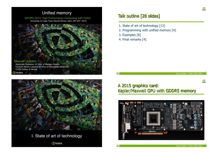
  1. Unified memory Talk outline [28 slides] GPGPU 2015: High Performance Computing with CUDA University of Cape Town (South Africa), April, 20 th -24 th , 2015 1. State of art of technology [12] 2. Programming with unified memory [4] 3. Examples [8] 4. Final remarks [4] Manuel Ujaldón Associate Professor @ Univ. of Malaga (Spain) Conjoint Senior Lecturer @ Univ. of Newcastle (Australia) CUDA Fellow @ Nvidia 2 A 2015 graphics card: Kepler/Maxwell GPU with GDDR5 memory I. State of art of technology 4

  2. A 2017 graphics card: The Pascal GPU prototype: Pascal GPU with 3D memory (stacked DRAM) SXM2.0 Form Factor 140 mm. SMX2.0*: 3x Performance Density 78 mm. (* Marketing Code Name. Name is not final). 5 6 Details on silicon integration Time to fill a typical cache line (128 bytes) 0ns. 20 ns. 40 ns. 60 ns. 80 ns. 100 ns. 120 ns. 140 ns. 160 ns. 180 ns. 200 ns. DRAM cells are organized in vaults , 100 MHz which take borrowed the interleaved Address bus Row Col. Tclk = 10 ns. memory arrays from already existing Control bus (burst length: 16 words of 8 bytes to complete a cache lines 128 bytes long) ACTIVE READ SDRAM-100, RCD=2 CL=2 Data bus Dato Dato Dato Dato Dato Dato Dato Dato Dato Dato Dato Dato Dato Dato Dato Dato CL=2 (1998) DRAM chips. t = 200 ns. Dato Dato Dato Dato Dato Dato Dato Dato DDR-200, CL=2 latency RCD=2 CL=2 A logic controller is placed at the base t = 120 ns. weight: 20% Dato Dato Dato Dato latency weight: 33% Dato Dato Dato Dato of the DRAM layers , with data matrices DDR-200, CL=2, dual-channel architecture RCD=2 CL=2 t = 80 ns. 200 MHz The most popular memory in 2015 is on top. latency weight: 50% DDR3-1600, with RCD=11 and CL=11. The assembly is connected with These two latencies represent 27.5 ns. out of 30 ns., 91.6% of the total time. through-silicon vias, TSVs , which DDR2-400, CL=4, RCD=4 CL=4 traverse vertically the stack using pitches We have been waiting more than dual-channel t = 60 ns. 15 years for this chance, and now between 4 and 50 um. with a vertical latency with TSVs in 3D it is real. weight: 66% latency of 12 picosecs. for a Stacked DDR2-400, CL=4, quad-channel t = 50ns. Latency weight: 80% RCD=4 CL=4 DRAM endowed with 20 layers. DDR3-800, CL=8, quad-channel t = 45 ns. Latency weight: 89% RCD=8 CL=8 7 8

  3. 3D integration, Using 3D chips to build a Haswell-like CPU side by side with the processor Step 5: Buses connecting 3D memory chips We have CPU, GPU and SRAM in different proportions Step 1: Partition into 16 cell and the processor are incorporated. matrices (future vaults) within silicon die, depending on 8 available models: Links to processor(s), which can be another 3D Vault control chip, but more interface Link heterogeneous: - Base: CPU y GPU. Step 4: Build vaults with TSVs - Layers: Cache (SRAM). A typical multi-core die Step 3: Pile-up Vault control uses >50% for SRAM. interface DRAM layers. Link And those transistors Cossbar switch Memory control switch slower on lower Logic base Step 2: Gather the voltage, so the cache will rely on interleaving common logic underneath. over piled-up matrices, Vault control just the way DRAM does. interface Link 3D technology 3D technology for DRAM memory for processor(s) DRAM7 SRAM7 Typical DRAM DRAM6 SRAM6 Vault control interface chips use 74% DRAM5 SRAM5 Link of the silicon DRAM4 SRAM4 DRAM3 SRAM3 area for the DRAM2 SRAM2 cell matrices. DRAM1 SRAM1 DRAM0 SRAM0 And, in addition, we want to include some DRAM layers. Control CPU+GPU logic 9 10 Intel already authored a research Today showing the best choices (*) Axiom: DRAM is 8 times more dense than a SRAM. Hypothesis: A core uses similar die area than 2 MB L3 (Ivy Bridge @ 22nm. fulfills this today if we left L2 aside). GPU CPU Evaluation: 2 layers, with the following alternatives (all PCIe reached similar temperatures): 16 GB/s Layer #1 Layer #2 Area Latency Bandwidth Power cons. Cache DRAM DRAM GDDR5 DDR4 2 cores + 4 MB L3 Empty 1+0 = 1 High High 92 W. 32 MB. 64 MB. 8 MB. 250-350 GB/s 50-75 GB/s 2 cores + 4 MB L3 8 MB L3 1+1 = 2 Medium Medium 106 W. Core 1 Core 1 Core 1 Core 1 Cache Cache Cache 2 cores 32 MB. DRAM 1/2+1/2=1 Low Low 4 MB. 88 W. 4 MB. 4 MB. Core 2 Core 2 Core 2 Core 2 2 cores + 4 MB L3 64 MB. DRAM 1+1 = 2 Very low Very low 98 W. GDDR5 Memory DDR4 Memory Alternative 1 Alternative 2 Alternative 3 Alternative 4 Given the higher role played by latency, the last row is the winner: DRAM is the greatest beneficiary of 3D integration. (*) B. Black et al. "Die Stacking (3D) Microarchitecture", published in MICRO'06. 11 12

  4. In four years: In two years All communications internal to the 3D chip 3D-DRAM Boundary of the GPU CPU silicon NVLINK die 80 GB/s SRAM DDR4 Memory stacked 100 GB/s in 4 layers: 1 TB/s GPU 2.5D memory DDR4 CPU 13 14 The idea: Accustom the programmer to see the memory that way CUDA 2007-2014 CUDA 2015 on CPU GPU CPU Maxwell GPU PCI-express Unified DDR3 GDDR5 DDR3 GDDR5 memory Main memory Video memory The new API: The old hardware Same memory, and software model: a single global Different memories, address space. II. Programming with unified memory performances Performance sensitive and address spaces. to data proximity. 15

  5. Unified memory contributions CUDA memory types Simpler programming and memory model: Zero-Copy Unified Virtual Unified Memory (pinned memory) Addressing Single pointer to data, accessible anywhere. CUDA call cudaMallocHost(&A, 4); cudaMalloc(&A, 4); cudaMallocManaged(&A, 4); Eliminate need for cudaMemcpy() . Allocation fixed in Main memory (DDR3) Video memory (GDDR5) Both Greatly simplifies code porting. Local access for CPU Home GPU CPU and home GPU PCI-e access for All GPUs Other GPUs Other GPUs Performance through data locality: Other features Avoid swapping to disk No CPU access On access CPU/GPU migration Migrate data to accessing processor. Coherency At all times Between GPUs Only at launch & sync. Guarantee global coherency. Full support in CUDA 2.2 CUDA 1.0 CUDA 6.0 Still allows cudaMemcpyAsync() hand tuning. 17 18 Additions to the CUDA API Unified memory: Technical details New call: cudaMallocManaged(pointer,size,flag) The maximum amount of unified memory that can be allocated is the smallest of the memories available on GPUs. Drop-in replacement for cudaMalloc(pointer,size) . Memory pages from unified allocations touched by CPU are The flag indicates who shares the pointer with the device: required to migrate back to GPU before any kernel launch. cudaMemAttachHost : Only the CPU. cudaMemAttachGlobal: Any other GPU too. The CPU cannot access any unified memory as long as GPU All operations valid on device mem. are also ok on managed mem. is executing, that is, a cudaDeviceSynchronize() call is New keyword: __managed__ required for the CPU to be allowed to access unified memory. Global variable annotation combines with __device__ . The GPU has exclusive access to unified memory when Declares global-scope migratable device variable. any kernel is executed on the GPU, and this holds even if the Symbol accessible from both GPU and CPU code. kernel does not touch the unified memory (see an example New call: cudaStreamAttachMemAsync() on next slide). Manages concurrently in multi-threaded CPU applications. 19 20

  6. First example: Access constraints __device__ __managed__ int x, y = 2; // Unified memory __global__ void mykernel() // GPU territory { x = 10; } int main() // CPU territory { mykernel <<<1,1>>> (); y = 20; // ERROR: CPU access concurrent with GPU return 0; } III. Examples 22 First example: Second example: Access constraints Sorting elements from a file __device__ __managed__ int x, y = 2; // Unified memory CPU code in C GPU code from CUDA 6.0 on __global__ void mykernel() // GPU territory { void sortfile (FILE *fp, int N) void sortfile (FILE *fp, int N) x = 10; { { } char *data; char *data; data = (char *) malloc(N); cudaMallocManaged(&data, N); int main() // CPU territory { mykernel <<<1,1>>> (); fread(data, 1, N, fp); fread(data, 1, N, fp); cudaDeviceSynchronize(); // Problem fixed! // Now the GPU is idle, so access to “y” is OK qsort(data, N, 1, compare); qsort<<<...>>>(data, N, 1, compare); y = 20; cudaDeviceSynchronize(); return 0; use_data(data); use_data(data); } free(data); cudaFree(data); } } 23 24

Download Presentation
Download Policy: The content available on the website is offered to you 'AS IS' for your personal information and use only. It cannot be commercialized, licensed, or distributed on other websites without prior consent from the author. To download a presentation, simply click this link. If you encounter any difficulties during the download process, it's possible that the publisher has removed the file from their server.

Recommend


More recommend