SYSC3601 Microprocessor Systems Unit 9: The Motorola 68000 P - - PowerPoint PPT Presentation

sysc3601 microprocessor systems unit 9 the motorola 68000
SMART_READER_LITE
LIVE PREVIEW

SYSC3601 Microprocessor Systems Unit 9: The Motorola 68000 P - - PowerPoint PPT Presentation

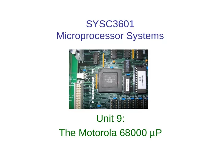
SYSC3601 Microprocessor Systems Unit 9: The Motorola 68000 P Topics/Reading 1. Overview of the 68000 P 2. Programming model, assembly, addressing modes, stack 3. 68000 Hardware interfacing, bus arbitration 4. Read/Write cycles 5. Memory


slide-1
SLIDE 1

SYSC3601 Microprocessor Systems Unit 9: The Motorola 68000 µP

slide-2
SLIDE 2

SYSC3601 2 Microprocessor Systems

Topics/Reading

  • 1. Overview of the 68000 µP
  • 2. Programming model, assembly, addressing modes, stack
  • 3. 68000 Hardware interfacing, bus arbitration
  • 4. Read/Write cycles
  • 5. Memory organization
  • 6. Memory interfacing
  • 7. I/O interfacing
  • 8. Exception processing, hardware interrupts

Reading: Antonakos, chapters 1,2,3,4,7,8,9,12

slide-3
SLIDE 3

SYSC3601 3 Microprocessor Systems

Motorola 68000 µP

  • 6800 µP - introduced in 1974, 8-bit.
  • 68000 µP - introduced in Sept 1979.

– NMOS (N-channel MOS technology) – 68K transistors? – 64 Pin DIP (8086 is 40) → No multiplexing. – Internal architecture is 32 bits (ALU is 16 bits wide). – 23 bit (physical) address bus A1-A23. No A0.

  • (24 bit effective address bus with LDS/UDS…)

– 16 bit data bus. – Operands:

  • Bytes
  • Words (16-bits)
  • Long words (32-bits)
slide-4
SLIDE 4

SYSC3601 4 Microprocessor Systems

Motorola 68000 µP

  • 68008 - 8 bit data bus, 20 bit address bus.
  • 68010 - 1982. Added virtual memory support.
  • 68020 - 1984. Fully 32 bit. 3 stage pipeline.

– 256 byte cache. More addressing modes!

  • 68030 - 1987. Integrated MMU into chip.
  • 68040 - 1991. Harvard architecture with two 4KB
  • caches. FP on chip. 6 stage pipeline.
  • 68060 - 1994. Superscalar version . 10-stage
  • pipeline. 2 integer, 1 fp unit. 8k caches. 4-5W.
  • Coldfire - 1995. Embedded version. Stripped
  • ut funky addressing modes.
slide-5
SLIDE 5

SYSC3601 5 Microprocessor Systems

Motorola 68000 µP

  • Used in:

– Apple Macintosh (then PPC, now Intel!!). – Atari 520ST and 1040ST (Defunct). – Amiga (Defunct). – Early Sun workstations (Now SPARC). – NeXT (Defunct, purchased by Apple 1996, MAC OS X came from ‘NeXTStep’).

  • 68000 architecture has user/supervisor

modes.

– protects operating system. – supports multitasking and multiprocessing.

slide-6
SLIDE 6

SYSC3601 6 Microprocessor Systems

Motorola 68000 µP – Programming Model

slide-7
SLIDE 7

SYSC3601 7 Microprocessor Systems

Motorola 68000 µP - Assembler

  • format: INST SRC,DST
  • Prexes:

– % binary – $ Hexadecimal – # Immediate.

  • Attach size to instruction, e.g.:

– move.b byte – move.w word – move.l long word

  • `()' refers to indirect addressing

– (recall that Intel uses `[]').

slide-8
SLIDE 8

SYSC3601 8 Microprocessor Systems

Motorola 68000 µP – Assembler Examples

  • move.b #$F5,d1

– Store immediate (#) hex ($) byte (.b), $F5 into destination d1. 8-bit transfer.

  • move.w (a2),d1

– stores contents of memory addressed by a2 into data register d1. 16-bit transfer.

  • add.l d4,d5

– Add 32-bit contents of register d4 to d5 and store the results in d5. Set flags.

slide-9
SLIDE 9

SYSC3601 9 Microprocessor Systems

Motorola 68000 µP – Addressing Modes

  • There are 14 different addressing modes (more with the 68020!)

Mode Syntax Data reg direct dn, n = 0..7 Addr reg direct an, n = 0..7 Addr reg indirect (an) with Postincrement (an)+ with Predecrement

  • (an)

with Displacement d16(an) with Index d8(an,Xm) (Xm is any am or dm) Relative with offset d16(PC) Relative with index and offset d8(PC,Xn) Absolute short < … > (16-bits sign-extended to 32) (for 000000-007FFF or FF8000-FFFFFF) Absolute long < … > (32-bits) Immediate #< … > Quick immediate #< … > (1 byte, sign-extend to 32) Implied Register specified as part of mnemonic

slide-10
SLIDE 10

SYSC3601 10 Microprocessor Systems

Motorola 68000 µP – Addressing Mode Examples

  • move.b #$6f,d0

– Immediate

  • move.w d3,d4

– data reg direct. Lower 16 bits of d3 are copied to low 16-bits of d4, upper d4 not changed

  • movea.l a5,a2

– address reg direct. Size must be .w or .l; .w implies sign extension

  • move.b (a0),d7

– address register indirect. Byte pointed at by a0 copied to d7

  • move.w (a5)+,d2

– post-increment. Word pointed at by a5 copied to d2, a5 then incremented by two (.w)

  • move.b -(a2),d4

– pre-decrement. a2 decremented by one, then byte pointed at by a2 copied to d4

slide-11
SLIDE 11

SYSC3601 11 Microprocessor Systems

Motorola 68000 µP – Addressing Mode Examples

  • move.w $100(a0),d0

– addr reg indirect with displacement. Contents of memory at a0+10016 copied to d0

  • move.b $08(a0,d1.w),d0

– addr reg indir with index. Note: can specify size here! Uses b15-b0 of d1 only (addr=a0+d1.w+$08)

  • move.b $9AE0,d1

– absolute short. Sign extend to get data from address $FF9AE0.

  • move.b $2E0000,d4

– Absolute long

  • moveq #$2C,d3

– Quick Immediate. Byte only (data encoded within instruction word). Byte is sign-extended to 32 bits.

slide-12
SLIDE 12

SYSC3601 12 Microprocessor Systems

Motorola 68000 µP – Addressing Mode Examples

  • Example: A sample assembler subroutine for the 68000:

Total: Find the sum of 16-bytes stored in memory.

  • rg

$8000 ;load program counter total clr.w d0 ;clear D0. move.b #16,d1 ;initialize counter movea.l #data,a0 ;init pointer to data loop add.b (a0)+,d0 ;add byte, increment address subq.b #1,d1 ;decrement counter bne loop ;test for zero, branch not equal. movea.l #sum,a1 ;load address to store result move.w d0,(a1) ;store sum at sum rts ;return from subroutine. sum dc.w 0 ;save room for result. data ds.b 16 ;save room for 16 data bytes. end

  • Note:

– dc.w - define a constant word, operand specifies the value to be written. – ds.b - define storage byte, operand specifies number of bytes, but not the contents

slide-13
SLIDE 13

SYSC3601 13 Microprocessor Systems

Motorola 68000 µP – Stack

  • Address register a7 is used to point to the stack.
  • There are no push or pop instructions

– (except for pea - push effective address).

  • A push is done with:

move.l d3,-(a7)

  • 1. Decrement a7 by four,
  • 2. Write 32 bits to stack
  • Actually implemented as:
  • 1. Decrement a7 by two.
  • 2. Write low word of d3
  • 3. Decrement a7 by two.
  • 4. Write high word of d3
slide-14
SLIDE 14

SYSC3601 14 Microprocessor Systems

Motorola 68000 µP – Stack

  • A pop is done with

move.l (a7)+,d3

  • Stack grows down (towards lower addresses)
  • pea - Push Effective Address.

pea $40(a5)

– Effective address is sum of a5 and $40. – Result is pushed.

  • jsr, rts - Subroutine calls

– Push/pop program counter and branch.

slide-15
SLIDE 15

SYSC3601 15 Microprocessor Systems

Motorola 68000 µP – Instruction Set

slide-16
SLIDE 16

SYSC3601 16 Microprocessor Systems

Motorola 68000 µP – Hardware

  • 16-bit µP - 16-bit data bus (D15-D0).

– Internal data paths are 32 bit

  • 24-bit address bus.

– ( UDS, LDS, A1-A23)

  • No multiplexing of busses!
  • Clock speeds of 4-12.5 MHz.

– 10/12/16/20 MHz for CMOS version (1/10th power consumption) Note that we will use ‘d7’ for data register d7 and ‘D7’ for data bus line D7. Likewise for a7 vs. A7.

slide-17
SLIDE 17

SYSC3601 17 Microprocessor Systems

Motorola 68000 µP – Hardware

Clock Circuit

Crystal

slide-18
SLIDE 18

SYSC3601 18 Microprocessor Systems

Motorola 68000 µP – Asynchronous bus control

  • AS Address strobe: valid address is on address

bus.

  • R/W: for read, 0 for write.
  • UDS: Upper data strobe. Data on D15-D8 (like BHE).
  • LDS: Lower data strobe. Data on D7-D0 (like BLE).
  • DTACK: Data transfer acknowledge.

– Signal by external hardware that µP may complete the current bus cycle. – During read, µP latches data when DTACK = 0. – During write, µP puts data on bus and keeps it there until DTACK = 0.

slide-19
SLIDE 19

SYSC3601 19 Microprocessor Systems

Motorola 68000 µP – Asynchronous bus control

slide-20
SLIDE 20

SYSC3601 20 Microprocessor Systems

Motorola 68000 µP – Hardware

  • System control

– RESET: reset the µP. (in) – HALT: µP puts the busses into high-impedance state

  • (Equivalent to HOLD on 8086) (in/out).

– BERR: Bus error - illegal memory location (in)

  • YOU must generate this if DTACK or VPA never returns
slide-21
SLIDE 21

SYSC3601 21 Microprocessor Systems

Motorola 68000 µP – Hardware

  • FC0, FC1, FC2:

– Encoded processor states. – only valid with AS = 0 (address strobe). – FC0FC1FC2 = 111: interrupt acknowledge.

  • IPL0, IPL1, IPL2

– Encoded interrupt priority level. – Seven interrupt levels. – Level 7 (all zeros) is highest

IACK

slide-22
SLIDE 22

SYSC3601 22 Microprocessor Systems

Motorola 68000 µP – Bus arbitration

  • Bus arbitration control:

– BR: Bus request (in) – BG: Bus grant (out) – BGACK: Bus grant acknowledgment (in)

  • Used to place 68000 busses in high

impedance state so that a peripheral can use the bus.

  • Sequence:
  • 1. External device sets BR = 0.
  • 2. 68000 sets BG = 0.
  • 3. External device waits for BG = 0, AS = 1,

DTACK = 1, BGACK = 1, then will set BGACK = 0 to take control of busses.

slide-23
SLIDE 23

SYSC3601 23 Microprocessor Systems

Motorola 68000 µP – Bus arbitration

slide-24
SLIDE 24

SYSC3601 24 Microprocessor Systems

Motorola 68000 µP – Hardware

  • Interface to 6800 peripherals:

– E: Clock (out) – VPA: Valid Peripheral address (in).

  • Should be asserted by interface circuitry whenever a 6800

peripheral has been selected.

– VMA: Valid Memory address (out).

  • Asserted by µP when internal clock is in synch with E-clock.

Connected to second peripheral CS pin.

1 2 3

slide-25
SLIDE 25

SYSC3601 25 Microprocessor Systems

Motorola 68000 µP – Fully Buffered 68000

slide-26
SLIDE 26

SYSC3601 26 Microprocessor Systems

Motorola 68000 µP – Read/Write Bus Cycles

  • The 68000µP uses AS=0 to signal a memory

access.

  • When memory sees AS=0, and it is the

correct address, it responds by pulling DTACK low which tells the µP to proceed with the data transfer.

  • Bus cycles are divided into a minimum of

eight states, S0 - S7. Each state is 1/2 a clock cycle.

slide-27
SLIDE 27

SYSC3601 27 Microprocessor Systems

Motorola 68000 µP – Read Cycle

  • S0: Address bus is in high impedance state, R/W is

set to 1 (read operation).

  • S1: Valid address appears on address bus.
  • S2: AS goes low (valid address), LDS and UDS are

set to the desired state.

  • S3,S4: Minimum time given to memory to signal

with DTACK=0.

  • S5: µP looks for DTACK=0.

– if DTACK=1, insert two wait states then test DTACK again. – if DTACK=0, continue with S6 and S7.

  • S6: Nothing new happens.
  • S7: Latch data into µP, set AS, UDS, and LDS to 1.

Memory releases DTACK

slide-28
SLIDE 28

SYSC3601 28 Microprocessor Systems

Motorola 68000 µP – Read Cycle

A1-A23

Data may not be avail when DTACK drops Only guaranteeing that it WILL be ready in time (end of S6) ASYNCHRONOUS! From memory device. READ DATA (end of S6) CHECK DTACK (S5) DTACK released when AS released

slide-29
SLIDE 29

SYSC3601 29 Microprocessor Systems

Motorola 68000 µP – Write Cycle

  • S0: Address bus is in high impedance state.
  • S1: Valid address appears on address bus.
  • S2: AS goes low (valid address), R/W is set to 0 (write
  • peration). (LDS and UDS are delayed to allow the bus

transceivers to switch direction, and to allow the memory time to prepare.)

  • S3: Valid data is placed on the bus by the µP.
  • S4: LDS and UDS are set to the desired state.
  • S5: µP looks for DTACK=0.

– if DTACK=1, insert two wait states then test DTACK again. – if DTACK=0, continue with S6 and S7.

  • S6: Nothing new happens.
  • S7: Set AS, UDS, and LDS to 1. Memory releases DTACK
slide-30
SLIDE 30

SYSC3601 30 Microprocessor Systems

Motorola 68000 µP – Write Cycle

A1-A23

ASYNCHRONOUS! From memory, can arrive any time before S5 without causing wait states

slide-31
SLIDE 31

SYSC3601 31 Microprocessor Systems

Motorola 68000 µP – Memory Organization

  • 68000 is byte-addressable.
  • 16-bit words and 32-bit long words must begin at

an even address, otherwise address error.

  • 68000 is a big-endian processor:

– 16-bit words are stored with the lower-order byte (endian) in the higher-order (big) memory address. – (Recall that the 8086 is little-endian)

  • Consequences:

Bank 8086 68000 D7-D0 Even (BLE) Odd (LDS) D15-D8 Odd (BHE) Even (UDS)

slide-32
SLIDE 32

SYSC3601 32 Microprocessor Systems

Motorola 68000 µP – Memory Organization

  • 8086 memory is usually drawn with odd bank on left, and

even bank on right.

  • 68000 memory is usually drawn with even bank on left,

and odd bank on right.

Odd Even 00003H HIGH LOW 00002H 00001H 00000H D15-D8 (BHE) D7-D0 (BLE) Even Odd $000002 HIGH LOW $0000003 $000000 $0000001 D15-D8 (UDS) D7-D0 (LDS)

slide-33
SLIDE 33

SYSC3601 33 Microprocessor Systems

Motorola 68000 µP – Memory Organization

  • Ex 68000 memory segment:

Even (High) Odd (Low) $00100A C3 8F $00100B $001008 3F 6B $001009 $001006 00 4A $001007 $001004 23 08 $001005

Byte@$1004 = $23 (high half) Byte@$1005 = $08 (low half) Word@$1006 = $004A (both halves) Word@$1008 = $3F6B (both halves) Word@$1009 = Address Error Long word@$1008 = $3F6BC38F (both halves, twice) Long word@$1005 = Address Error

slide-34
SLIDE 34

SYSC3601 34 Microprocessor Systems

Motorola 68000 µP – Memory Interfacing

  • Almost identical to the 8086 except:
  • 1. Switch even and odd banks
  • 2. Must generate DTACK
  • 3. Must use AS, R/W, UDS and LDS for control.
  • During a byte-read operation, the µP will select

the correct half of the data bus depending on whether it's an even or odd address (similar to 8086). (However, most designs provide separate read strobes for even and odd banks.)

  • Separate write strobes are required for even and
  • dd banks so that data is not written to the

wrong memory bank.

slide-35
SLIDE 35

SYSC3601 35 Microprocessor Systems

Motorola 68000 µP – Memory Interfacing

  • Block diagram of DTACK circuit:
  • DTACK delay generator:

Note that AS high leads to DTACK going high immediately

‘Device select’ signal from address decoder. (goes low end of S1) ‘PRE’ presets the flip-flop (sets it to 1) Goes low on rising edge of S4 Goes low on rising edge of S6 (too late, causes 1 clock cycle delay)

slide-36
SLIDE 36

SYSC3601 36 Microprocessor Systems

Motorola 68000 µP – I/O Interfacing

  • All I/O is memory-mapped.
  • Decoding is the same as for memory.
  • One still must generate DTACK.

Would require another buffer/latch pair for UDS for a 16-bit I/O interface. (connected to D15-D8).

slide-37
SLIDE 37

SYSC3601 37 Microprocessor Systems

Motorola 68000 µP – Exceptions (Interrupts)

  • The 68000 has three execution states:
  • 1. Normal - running user program.
  • 2. Halted - not executing instructions. (perhaps

because of a system failure such as a double bus fault, or due to HALT pin).

  • 3. Exception (processing) state - includes

interrupts, but goes beyond the usual notion

  • f interrupts.
slide-38
SLIDE 38

SYSC3601 38 Microprocessor Systems

Motorola 68000 µP – Exceptions (Interrupts)

  • Two privilege states.

– User and Supervisor. – Some instructions are only available in supervisor state.

  • STOP, RESET, RTE, MOVE/AND/EOR/OR to SR,

MOVE to USP

– Separate stack pointers. – Provides security for operating systems etc. – All exception processing is done in supervisor state. – The only way to get to supervisor state is through an exception (or reset).

slide-39
SLIDE 39

SYSC3601 39 Microprocessor Systems

Motorola 68000 µP – Exceptions (Interrupts)

  • Can use privilege state for memory

management

– i.e. include FC2-pin in memory interface.

slide-40
SLIDE 40

SYSC3601 40 Microprocessor Systems

Motorola 68000 µP – Exceptions (Interrupts)

  • Interrupt Vectors and the vector table

– A vector number is one byte (0-255) – Vector Table:

  • Occupies the first 1kbyte (000-3FF) of memory.
  • Each entry (except the first) is a 32-bit address

pointing to the start of the exception handler code.

PC: Byte 3 Byte 2 Byte 1 Byte 0

$3FF … $017 PC7-PC0 Byte0 $016 PC15-PC8 Byte1 $015 PC23-PC16 Byte2 $014 PC31-PC24 Byte3 … $000

Ex: Vector = $5 (Divide by zero) 68000 fetches new PC From address $5 x 4 = $014 BIG Endian!!

slide-41
SLIDE 41

SYSC3601 41 Microprocessor Systems

Motorola 68000 µP – Exceptions (Interrupts)

slide-42
SLIDE 42

SYSC3601 42 Microprocessor Systems

Motorola 68000 µP – Exceptions (Interrupts)

  • Exception Processing Sequence
  • 1. Save the status register in a temporary

register and set the S-bit so that the 68000 can enter supervisor mode.

  • 2. Get the vector number. There are

several ways:

(a) may be determined internally by processor. (b) external interrupts can be “auto-vectored“ (to come). (c) external interrupts can provide a vector number (i.e. type) on D7-D0 during the interrupt acknowledge cycle.

slide-43
SLIDE 43

SYSC3601 43 Microprocessor Systems

Motorola 68000 µP – Exceptions (Interrupts)

  • 3. Save processor information onto supervisor

stack:

(a) push PC low word. (b) push PC high word. (c) push status register (from saved temporary unmodified version).

  • 4. Fetch new PC from the vector table.
  • 5. Execute exception handler.
  • 6. Return with RTE. Pops SR, then PC.
  • Note: Exceptions can be nested – not masked

automatically like 8086 does.

slide-44
SLIDE 44

SYSC3601 44 Microprocessor Systems

Motorola 68000 µP – Exceptions (Interrupts)

  • 68000 Hardware Interrupts

– Seven levels of external interrupts depending on IPL2, IPL1, and IPL0. – Level 0, all IPLs = 1, no interrupt. – Level 7, all IPLs = 0, highest priority (non-maskable). – Interrupt priority mask (bits 8, 9, and 10 of SR) is set to disable lower priority interrupts.

Example circuit to generate a level-7 interrupt using a single push-button. We can develop more complex circuits to generate multiple interrupt levels depending on the source

  • f the interrupt request.
slide-45
SLIDE 45

SYSC3601 45 Microprocessor Systems

Motorola 68000 µP – Exceptions (Interrupts)

  • Interrupt Acknowledge Cycle

– (asynchronous, hardware interrupt requests)

  • 1. Device and interrupt logic set IPL2, IPL1and

IPL0.

  • 2. µP completes current instruction.
  • 3. µP enters interrupt acknowledge cycle.

(a) FC2, FC1, FC0 = 111. (b) AS = 0, LDS = 0, R/W = 1. A3, A2, A1 = requested interrupt level.

slide-46
SLIDE 46

SYSC3601 46 Microprocessor Systems

Motorola 68000 µP – Exceptions (Interrupts)

  • Interrupt Acknowledge Cycle con’t
  • 4. External logic may do one of two things:

(a) Supply a vector number.

– Place 8-bit vector number of D7-D0. – pull DTACK low. – µP will read D7-D0.

(b) Request an “auto-vector".

– Pull VPA low. Leave DTACK high. – µP generates its own vector based on interrupt level first supplied to IPL inputs. – autovectors point to locations $064 through $07F in vector table.

– Autovectors should be used whenever 7 or less interrupt types are needed.

  • 5. Proceed with exception handling steps from slide 42
slide-47
SLIDE 47

SYSC3601 47 Microprocessor Systems

Motorola 68000 µP – Exceptions (Interrupts)

The response to an interrupt is quite lengthy and complex: 1. Resolve priorities from external interrupt request, present appropriate 3-bit code on IPL2-0 2. Monitor FC2-0 for intr acknowledge cycle.

  • AS=0,
  • R/W=1,
  • LDS=0
  • A3-1 = requested interrupt level

3. Either: 3a) provide vector number on D7-0 and pull DTACK low, OR 3b) request autovector by pulling VPA low. 1 1 2 2 2 2 3a 3a 3b 2

slide-48
SLIDE 48

SYSC3601 48 Microprocessor Systems

Motorola 68000 µP – Peripheral chips

68681 DUART

  • Contains 2 UARTs, independently programmable
  • Both channels can provide simultaneous

Tx/Rx.

  • Interface using internal control/data/status

registers selected via RS4-1 pins.

  • Also provides 6 parallel inputs and 8 parallel
  • utputs
  • Can be used for handshaking signals or

standard I/O pins.

slide-49
SLIDE 49

SYSC3601 49 Microprocessor Systems

Motorola 68000 µP – Peripheral chips

68230 Parallel Interface/Timer (PI/T)

  • Contains 3 8-bit parallel ports
  • Can be input, output, bidirectional
  • Ports A&B can form 16-bit port
  • Also contains an internal 24 bit timer
  • Count down, square wave generator,

etc.

  • 23 internal data/control/status registers

selected via RS5-1 pins.

  • H4-1 pins are handshaking for ports A&B
  • Can cause interrupts
  • PortC can be used as general I/O pins,

interrupt request/acknowlege, timer inputs/outputs, or DMA request.

slide-50
SLIDE 50

SYSC3601 50 Microprocessor Systems

Motorola 68000 µP – Peripheral chips

Keyboard scanning with a 68230 PI/T

  • Drive PA3-0 in sequence
  • Read PB3-0 to check for key depressed
slide-51
SLIDE 51

SYSC3601 51 Microprocessor Systems

Motorola 68000 µP – Peripheral chips

4 Digit Display with a 68230 PI/T

  • Select segments using PA7-0
  • Select display chip using PB3-0
  • Have to scan through chips quickly

to avoid flicker effect.

  • Use timer to cause interrupts to cycle

through chips.

slide-52
SLIDE 52

SYSC3601 52 Microprocessor Systems

Motorola 68000 µP – Peripheral chips

68881 Math co-processor

  • Similar to 8087
  • 8 Internal 80-bit floating point registers
  • 40 floating point instructions
  • 32-bit data bus
  • Optimally used with 68020 (32-bit bus)
  • A0 and SIZE are used to configure the 68881

for the size of the µP’s data bus.

slide-53
SLIDE 53

SYSC3601 53 Microprocessor Systems

Other peripheral chips: 68153 BUS Interrupt Module 68440 Dual DMA Controller 6851 Memory Management Unit 68901 Multifunction Peripheral 68465 Floppy Disk Controller 68452 Bus Arbitration Module 68590 LAN Controller for Ethernet 68652 Multiprotocol Communications Controller 68824 Token-Passing Bus Controller 68486/68487 Raster Memory System 68184 Broadband Interface Controller

Motorola 68000 µP – Peripheral chips

INTEL 8279 Keyboard/Display Chip

  • For non-68000 series chips, must

generate DTACK signal using interface circuitry.

  • Must also create separate RD

and WR signals from joint R/W