SLIDE 1 Physics, POSTECH
Quantum Transport and Superconductivity Laboratory Center for Topological Matter
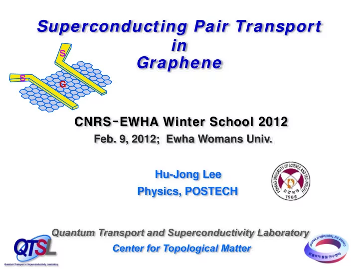
Hu-Jong Lee
G S S
CNRS-EWHA Winter School 2012
- Feb. 9, 2012; Ewha Womans Univ.
Superconducting Pair Transport in Graphene
SLIDE 2 Outline
1. Pair transport in S–mono-layer graphene–S junctions
– Basic concept – graphene and Josephson coupling – Pair transport in graphene
- 2. Switching current distribution in mono-layer GJJs
– Basic concept – switching current distribution – Gate tuning of different switching regimes – MQT, TA, PD – Observation of quantized levels in washboard potential
- 3. Top-gated bilayer GJJs
– E-field-induced band gap opening – S-I transition in top-gated bilayer GJJs
- 4. Josephson coupling across a graphene p-n potential barrier
– Klein tunneling of Cooper pairs
SLIDE 3
Carbon Allotropes : in Diverse Dim ensions
Two dimension Three dimension One dimension Zero dimension Patterning Functionality
SLIDE 4 1
a
2
a
Graphene
2.46 A
°
‘A’ sublattice ‘B’ sublattice
graphene lattice
(real space) Two equivalent sublattices Two atoms per unit cell π-orbital σ-bond SP2 covalent hybrid
π σ
SLIDE 5
- Dirac cone
- Linear dispersion at zero energy
Band Structure and Low -Energy Dispersion
- Massless relativistic Dirac fermions
- But moving with Fermi velocity
- Carrier type and density are easily controlled by gating
F
υ
F
E k υ = r h
K M Γ K’
EF
SLIDE 6
Chirality or Pseudospin in Graphene Lattice
pseudospin or chirality
K K’
kx ky kx E E
Chirality – momentum-locked phase value of a carrier in graphene when the carrier moves along a Dirac cone (or the sublattice index) electron-like hole-like
SLIDE 7
natural graphite
Graphene Preparation – Mechanical Exfoliation
exfoliated graphene on Si sub
1 3
10 μm
2
thin graphite on tape transferring graphene onto Si substrate
SLIDE 8
Graphene Preparation – Mechanical Exfoliation
10 μm 10 μm 10 μm 10 μm
SLIDE 9 1. Pair transport in S–mono-layer graphene–S junctions
– Basic concept – graphene and Josephson coupling – Pair transport in graphene
- 2. Switching current distribution in mono-layer GJJs
– Basic concept – switching current distribution – Gate tuning of different switching regimes – MQT, TA, PD – Observation of quantized levels in washboard potential
- 3. Top-gated bilayer GJJs
– E-field-induced band gap opening – S-I transition in top-gated bilayer GJJs
- 4. Josephson coupling across a graphene p-n potential barrier
– Klein tunneling of Cooper pairs
SLIDE 10 Josephson relations;
; Josephson coupling strength ; SC strength in electrodes
High-freq. Josephson oscillation;
V
L
S
R
S
L
ψ
R
ψ
I
I
Josephson Effect
Δ
c
I
SLIDE 11
- Finite supercurrent for d < ξ
- Supercurrent is carried either by electron-like carriers in the conduction band
- r by hole-like carriers in the valence band
S S G
Graphene-based Josephson Junction
Heersche et al., Nature 446 56 (2007)
SC Paring Condition;
- opposite momentum (k, -k) in two different valleys
- opposite spins ( )
K K’
SLIDE 12
- Josephson coupling is modulated by backgating
- Al electrodes; low Tc (=1.2 K)
small gap Δ (=0.17 meV)
- Josephson device applications ; higher-gap electrodes are required
S S G
Supercurrent in Graphene – Josephson Effect
Heersche et al., Nature 446 56 (2007)
SC Paring Condition;
- opposite momentum (k, -k) in two different valleys
- opposite spins ( )
Heersche et al., Nature 446 56 (2007) Al-G-Al CNP
+1 V
Vbg= -50 V
SLIDE 13 Pb0.93In0.07–G–Pb0.93In0.07 junction
- PbIn/Au (200/10 nm)
- spacing btw electrodes = 300 nm
monolayer graphene μ = 1400 cm2/Vs @ Vbg=-50 V Tc = 7 K
Sam ple PbI n-G-PbI n Junction
T = 6 mK H = 4.2 kG Finite resistance at VCNP
SLIDE 14
1 2 3
100 200
I (μA) V (μV) V
bg= -60 V
PbIn–G–PbIn Junction
Hysteresis in I V Characteristics
- IV curve is hysteretic – underdamped tunneling JJ
- Finite carrier diffusion time effective capacitance
VCNP=- 4 V
Carrier diffusion time;
2 D N eff
L R C D τ = =
2 eff N
L C R D = =
Effective junction capacitance;
10 - 80 fF
SLIDE 15
- Supercurrent is gate-voltage dependent
- Asymmetry by the hysteresis
PbIn–G–PbIn Junction Jc(0) ~ 9.4×10⁻³ A/cm ; record high
VBG Dependence of I c
Heersche et al., Nature 446 56 (2007) Al-G-Al Gate-voltage dependence of Ic
VCNP=- 4 V
SLIDE 16
- Supercurrent is gate-voltage dependent
- Asymmetry by the hysteresis
PbIn–G–PbIn Junction
T Dependence of I c
Gate-voltage dependence of Ic
VCNP=- 4 V
T dependence of Ic
SLIDE 17 Gate-voltage-dependent supercurrent
I c vs VBG
Proximity junction with diffusive N layer
- Variation of Ic should follow Gn
- Ic does not vanish even at the CNP
- R does not diverge at the CNP
I (μA) V (μV)
200
3 V
bg= -60V
10 5 15
G (mS) Ambegaokar-Baratoff relation
SLIDE 18 S S S S S S
Magnetic-Field Modulation of I c ( Fraunhofer Pattern)
- Fraunhofer pattern - Ic is modulated by a magnetic field
- Distribution of screening current varies with magnetic field
SLIDE 19 Shapiro steps - Cooper pairs tunneling in resonance with microwaves
Microw ave Response of JJ – Shapiro Steps
Vbg
Vertical current steps;
1 2 3
n=0 1 2
n=0
- D. Jeong et al., Phys. Rev. B 83, 094503 (2011)
SLIDE 20 Shapiro steps - Cooper pairs tunneling in resonance with microwaves
Microw ave Response of JJ – Shapiro Steps
2 ( )
n n
e I J hf Δ ∝ 2 h e
slope ~ 2.07 μV/GHz =2.12 μV/GHz
dV/dI (a.u.) P1/2 (a.u.) I (μA)
∆Vbg = 60 V
3
1 1 2 2 3 4
n=0
n=0 1 2 3
Vertical current steps;
SLIDE 21
Conductance peak at
Multiple Andreev Reflection
Δ=1.1 meV; close to the value of 1.35 meV of bulk Pb n = 3 n= +1, +2, +3…..
SLIDE 22 1. Pair transport in S–mono-layer graphene–S junctions
– Basic concept – graphene and Josephson coupling – Pair transport in graphene
- 2. Switching current distribution in mono-layer GJJs
– Basic concept – switching current distribution – Gate tuning of different switching regimes – MQT, TA, PD – Observation of quantized levels in washboard potential
- 3. Top-gated bilayer GJJs
– E-field-induced band gap opening – S-I transition in top-gated bilayer GJJs
- 4. Josephson coupling across a graphene p-n potential barrier
– Klein tunneling of Cooper pairs
SLIDE 23 : Phase particle
Josephson Junction - W ashboard Potential
current-biased RCSJ model washboard potential
Voltage (V) Current (I)
IV characteristics
SLIDE 24 Voltage (V) Current (I)
Potential Barrier
TA
Γ
MQT
Γ
Josephson Junction - W ashboard Potential
- Switching probability; SC state is switched
to resistive state in a stochastic way
P current-biased RCSJ model
SLIDE 25
Temperature, T Distribution Width of P(I)
; thermal activation ; MQT (independent of T)
Therm al Activation vs MQT
Switching Rate;
~ several tens GHz
; plasma frequency
P
SLIDE 26
Phase particle in single JJs Phase particle in stacked JJs Wallraff et al., Nature, 2003 Lee et al., PRB, 2010 Voss et al., PRL, 1981 Devoret et at, PRL, 1985 Inomata et al., PRL, 2005 Jin et al., PRL, 2006 Ueda et al., APL, 2007 Bae et al., PRB, 2009 MQT of a single vortex
A Few of Previous Studies
Jeong et al., PRB, 2011 Lee et al., PRL, 2011 This work; in gate-controlled graphene-based JJs
SLIDE 27 Sw itching Current Distribution P( I c)
I P
1 2 3 4 5 6 1 2
0.09 K 0.16 K 2.20 K 2.40 K 2.00 K 1.80 K 1.50 K 0.68 K 0.85 K 1.20 K 1.00 K 0.26 K
Counts/10
3
I ( μ A )
0.05 K 0.51 K
Vbg = -60 V
; Phase Diffusion (PD) ; Thermal Activation (TA) ; MQT
100 200 5.6 5.8 6.0 6.2
I (μA) V (μV) 100 switching events PD TA MQT
SLIDE 28 Sw itching Current Distribution Aw ay from DP
MQT TA PD
2/3
T σ ∝
1 2 3 4 5 6 1 2
0.09 K 0.16 K 2.20 K 2.40 K 2.00 K 1.80 K 1.50 K 0.68 K 0.85 K 1.20 K 1.00 K 0.26 K
Counts/10
3
I ( μ A )
0.05 K 0.51 K
Vbg = -60 V
; Phase Diffusion (PD) ; Thermal Activation (TA) ; MQT
PD TA MQT
SLIDE 29 Fulton and Dunkleberger, PRB 9, 4760 (1974)
1
( ) ( ) [1 ( ') ']
c
I c c
P I I I P I dI
−
= Γ −∫
1 2 3 4 5 6 10
2
10
3
10
4
10
5
Γ (s
I (μA)
}
} }
PD TA MQT PD TA MQT
SLIDE 30 0.3 0.6 0.9 1.2 0.0 0.5 1.0 1.5
Counts/10
3
I (μA)
Vbg = 0 V
} }
PD TA MQT
}
0.1 1 0.02
SD/Ic0 T (K)
0.028
Vbg = 0 V MQT TA PD
Sw itching Current Distribution near DP
SLIDE 31 Vbg = -60 V
0.1 1 0.02
SD/Ic0 T (K)
0.028
Vbg = -60 V
P( I c) Near and Aw ay from DP
0.3 0.6 0.9 1.2 0.0 0.5 1.0 1.5
Counts/10
3
I (μA)
Vbg = 0 V
SLIDE 32 }
}
}
PD TA MQT
1
( ) ( ) [1 ( ') ']
c
I c c
P I I I P I dI
−
= Γ −∫
0.3 0.6 0.9 1.2 0.0 0.5 1.0 1.5
Counts/10
3
I (μA)
Vbg = 0 V
} }
PD TA MQT
}
SLIDE 33 0.05 0.1 0.5 1 5 0.01 0.02
SD/Ic0 T (K)
Vbg Dependence of Different Escaping Regim es
- Different regimes are identified in a single SGS junction by varying the carrier
density in graphene using Vbg
Gil-Ho Lee, D. Jeong, J.-H. Choi, Y.-J. Doh, and H.-J. Lee, PRL 107, 146605 (2011)
PD TA MQT T = 6 mK H = 4.2 kG
Vbg = 0 V Vbg = -60 V
T*MQT T*TA
SLIDE 34 PD TA MQT 0.05 0.1 0.5 1 5 0.01 0.02
SD/Ic0 T (K)
T*MQT T*TA
Vbg = -60 V
Vbg = 0 V
Vbg Dependence of Different Escaping Regim es
- Different regimes are identified in a single SGS junction by varying the carrier
density in graphene using Vbg
Gil-Ho Lee, D. Jeong, J.-H. Choi, Y.-J. Doh, and H.-J. Lee, PRL 107, 146605 (2011)
PD TA MQT
Vbg-T phase diagram of GJJ
SLIDE 35
PD TA MQT
Vbg-T phase diagram of GJJ
SLIDE 36 }
Energy Level Quantization Probed by MW Excitation
}
}
in the MQT regime
Gil-Ho Lee et al., PRL 107, 146605 (2011)
n = 4 n = 10 5 6 7 8 9
Ir
SLIDE 37
Possible Realization of Defect-free Qubits
Two-level systems (TLS) in amorphous materials
L R
unwanted resonator
ωr
R.W. Simmonds …., PRL 93, 077003 (2004)
TLS gives unwanted resonance with qubit and additional decoherence.
Single crystalline graphene is free from TLS.
SLIDE 38
- Different escaping regime, MQT, TA, PD, of phase particles
are accessed by simply varying backgate voltage in a single GJJ.
- Transition between different energy levels by multiphoton
absorption
- Promissing for new quantum information device application
using graphene –based JJ
Sum m ary
SLIDE 39 1. Pair transport in S–mono-layer graphene–S junctions
– Basic concept – graphene and Josephson coupling – Pair transport in graphene
- 2. Switching current distribution in mono-layer GJJs
– Basic concept – switching current distribution – Gate tuning of different switching regimes – MQT, TA, PD – Observation of quantized levels in washboard potential
- 3. Top-gated bilayer GJJs
– E-field-induced band gap opening – S-I transition in top-gated bilayer GJJs
- 4. Josephson coupling across a graphene p-n potential barrier
– Klein tunneling of Cooper pairs
SLIDE 40
Lecture will be given for this subject but the note will not provided because the content is currently in preparation for publication.
SLIDE 41 1. Pair transport in S–mono-layer graphene–S junctions
– Basic concept – graphene and Josephson coupling – Pair transport in graphene
- 2. Switching current distribution in mono-layer GJJs
– Basic concept – switching current distribution – Gate tuning of different switching regimes – MQT, TA, PD – Observation of quantized levels in washboard potential
- 3. Top-gated bilayer GJJs
– E-field-induced band gap opening – S-I transition in top-gated bilayer GJJs
- 4. Josephson coupling across a graphene p-n potential barrier
– Klein tunneling of Cooper pairs
SLIDE 42
Lecture will be given for this subject but the note will not provided because the content is currently in preparation for publication.
SLIDE 43
Korea Univ.
KRICT
G.-H. Lee
Acknow ledgm ent
This work was supported by National Research Foundation through SRC – Center for Topological Matter
PbIn junction S-I transition Bipolar junction Switching current distribution
Andreev Spectroscopy
SLIDE 44
n=1 n=2 n=3 n=4 n=5 Conductance peak at