
SLIDE 1
Storage Class Memory Towards a disruptively low-cost solid-state - - PowerPoint PPT Presentation
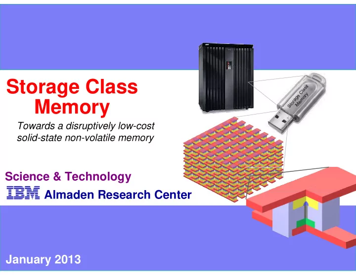
Storage Class Memory Towards a disruptively low-cost solid-state non-volatile memory Science & Technology Almaden Research Center January 2013 Storage Class Memory Power & space in the server room The cache/memory/storage hierarchy
Storage Class Memory
2
Science & Technology – IBM Almaden Research Center
Jan 2013
The cache/memory/storage hierarchy is rapidly becoming the bottleneck for large systems. We know how to create MIPS & MFLOPS cheaply and in abundance, but feeding them with data has become the performance-limiting and most-expensive part of a system (in both $ and Watts).
(at 70% CGR need
2 GI OP/ sec)
system technology –"Storage Technologies & Systems" special issue
Storage Class Memory
3
Science & Technology – IBM Almaden Research Center
Jan 2013
(at 90% CGR need 8.4G SI O/ sec)
Typical Examples:
Analyze petabytes of data
Search and Mining Analyses of social/terrorist networks Sensor network processing Digital media creation/transmission Environmental & economic modeling
Solve differential equations
Computational Fluid Dynamics Finite Element Analysis Multi-body Simulations (at 90% CGR need 1.7 PB/ sec)
[Freitas:2008]
Storage Class Memory
4
Science & Technology – IBM Almaden Research Center
Jan 2013
ON-chip memory OFF-chip memory ON-line storage OFF-line storage
Decreasing co$t
100 108 103 104 105 106 107 109 1010
Get data from DRAM/SCM (60ns)
10
1
CPU operations (1ns) Get data from L2 cache (<5ns) Read or write to DISK (5ms) Get data from TAPE (40s) ...(in human perspective)
(T x 109) second minute hour day week month year decade century millenium
Access time... (in ns)
between memory and storage caching, threads, predictive branching, etc.
retrieval of data from off-line tape represents an analogous delay of 1250 years
Storage Class Memory
5
Science & Technology – IBM Almaden Research Center
Jan 2013
and storage capacities are increasing as devices scale down to smaller dimensions…
FLASH SSD
…but while prices are dropping, the performance gap between memory and storage remains significant, and the already-poor device endurance of Flash is getting worse.
ON-chip memory OFF-chip memory ON-line storage OFF-line storage
Decreasing co$t
100 108 103 104 105 106 107 109 1010
Get data from DRAM/SCM (60ns)
10
1
CPU operations (1ns) Get data from L2 cache (<5ns) Read or write to DISK (5ms) Get data from TAPE (40s)
Access time... (in ns)
Write to FLASH, random (1ms) Read a FLASH device (20 us)
Memory/storage gap
Storage Class Memory
6
Science & Technology – IBM Almaden Research Center
Jan 2013
Research into new solid-state non-volatile memory candidates – originally motivated by finding a “successor” for NAND Flash – has opened up several interesting ways to change the memory/storage hierarchy…
ON-chip memory OFF-chip memory ON-line storage OFF-line storage
Decreasing co$t
100 108 103 104 105 106 107 109 1010
Get data from DRAM/SCM (60ns)
10
1
CPU operations (1ns) Get data from L2 cache (<5ns) Read or write to DISK (5ms) Get data from TAPE (40s)
Access time... (in ns)
Write to FLASH, random (1ms) Read a FLASH device (20 us)
Memory/storage gap
1) Embedded Non-Volatile Memory – low-density, fast ON-chip NVM 2) Embedded Storage – low density, slower ON-chip storage 3) M-type Storage Class Memory – high-density, fast OFF- (or ON* )-chip NVM 4) S-type Storage Class Memory – high-density, very-near-ON-line storage
* ON-chip using 3-D packaging
Storage Class Memory
7
Science & Technology – IBM Almaden Research Center
Jan 2013
The cost basis of semiconductor processing is well understood – the paths to higher density are 1) shrinking the minimum lithographic pitch F, and 2) storing more bits PER 4F2
F F 4F2
Storage Class Memory
8
Science & Technology – IBM Almaden Research Center
Jan 2013
component failure or loss of power) requires
redundancy in system architecture
(process-, thread-switching)
~ 1us read latency
Storage Class Memory
9
Science & Technology – IBM Almaden Research Center
Jan 2013
High Speed Low co$t
Embedded Non-Volatile Memory
(low-density, fast ON-chip NVM)
Embedded Storage
(low density, slower ON-chip storage)
Future NOR applications
(program code, etc.)
Future NAND applications
(consumer devices, etc.)
conventional NAND may require > 50 layers!)
M-type Storage Class Memory
(high-density, fast OFF- (or ON* )-chip NVM)
S-type Storage Class Memory
(high-density, very-near-ON-line storage) 1) PCM?/ RRAM? 2) Racetrack? (future?)
* ON-chip using 3-D packaging
Storage Class Memory
10
Science & Technology – IBM Almaden Research Center
Jan 2013
Device Availability
Embedded Storage
(low density, slower ON-chip storage)
S-type SCM
(high-density, near-ON-line storage)
emerging NVM
RRAM? PCM? CBRAM?
* ON-chip using 3-D packaging
M-type SCM
(high-density, fast OFF-(or ON* )
Embedded
Non-Volatile Memory
(low-density, fast ON-chip NVM)
emerging NVM
STT-RAM? CBRAM? PCM??/ RRAM??
(working memory, etc.)
Capital investment Applications
3-D NAND
(consumer devices, etc.)
Co$t
unlikely, but possible path
Storage Class Memory
11
Science & Technology – IBM Almaden Research Center
Jan 2013
NVM memory element plus access device
Storage Class Memory
12
Science & Technology – IBM Almaden Research Center
Jan 2013
Asymmetric performance Writes much slower than reads Program/erase cycle Block-based, no write-in-place Data retention and Non-volatility Retention gets worse as Flash scales down
17 60 200 7 40 100 1 10 100 1000 USB disk LapTop Enterprise MB/s
Sustained Read Bandwidth Sustained Write Bandwidth
2000 10000 52000 49 17000 3000 10 100 1000 10000 100000 USB disk LapTop Enterprise IOPS
Maximum Random Read IOPs Maximum Random Write IOPs
Endurance
Future outlook
Storage Class Memory
13
Science & Technology – IBM Almaden Research Center
Jan 2013
magnetic tunnel junction using current, leading to two distinct resistance states
Bit Line Plate Line Word Line
While near-term prospects for high-density SCM with STT-RAM may seem dim, Racetrack Memory offers hope for using STT concepts to create vertical “shift-register” of domain walls potential densities of 10-100 bits/F2
Storage Class Memory
14
Science & Technology – IBM Almaden Research Center
Jan 2013
‘heater’ wire insulator
word line bit line
access device
and high-resistance amorphous phases, controlled through power & duration of electrical pulses
To keep switching power down sub-lithographic feature and high-current Access Device To fill small feature ALD or CVD difficult now to replace GST with a better material Variability in small features broadens resistance distributions
drift-mitigation and/or 3-D Access Devices can offer high-density (= low-cost), then
Storage Class Memory
15
Science & Technology – IBM Almaden Research Center
Jan 2013
RESET
Voltage-controlled formation & dissipation of an oxygen-vacancy (or metallic) filament through an otherwise insulating layer
but then requires an unconventional bipolar-capable Access Device (transistor or diode is out)
yield & reliability could focus industry efforts considerably. Absent that, many uncertainties remain about prospects for reliable storage & memory products.
Top electrode
Bottom electrode
“Forming” step
SET
Conductive filament
Storage Class Memory
16
Science & Technology – IBM Almaden Research Center
Jan 2013
NVM memory element plus access device
Storage Class Memory
17
Science & Technology – IBM Almaden Research Center
Jan 2013
Effective cell size: 4F2 Effective cell size: 4F2/ L
Stack ‘L’ layers in 3D
F = minimum litho. feature size
As a result of the cost-basis of semiconductor manufacturing, memory cost is inversely related to bit density
Since they effectively store more bits per 4F2 footprint,
(adapted from Burr, EIPBN 2008)
Storage Class Memory
18
Science & Technology – IBM Almaden Research Center
Jan 2013
incorrect sensing and wasted power
Storage Class Memory
19
Science & Technology – IBM Almaden Research Center
Jan 2013
PCM or RRAM Access Device
wide low-leakage (< 100pA) voltage zone to accommodate half-selected cells in large arrays
needed for optimum RRAM operation
Storage Class Memory
20
Science & Technology – IBM Almaden Research Center
Jan 2013
100A 1A 100nA 10nA 1nA 100pA 10pA 0.3 0.1
Applied Voltage
[V]
1pA 10A 0.5
W
gap
W
gap
W=200nm Gap=100nm Overlap=250nm
200nm inert TEC 80nm BEC
10A 1A 100nA 10nA 1nA 100pA 10pA 1pA 100A
0.2 0.4 0.6 0.8
Voltage [V]
MIEC TEC
ILD BEC poly-Si series resistor
MIEC TEC
ILD BEC poly-Si series resistor
(Gopalakrishnan et al, 2010 VLSI Tech. Sym.)
Storage Class Memory
21
Science & Technology – IBM Almaden Research Center
Jan 2013
As-deposited Post-CMP TEM x-section 180 nm CMOS Front-End 1T-1MI EC
(1 transistor + 1 MI EC access device)
CMP process for MIEC material with modified commercial Cu slurry
(Shenoy et al, 2011 VLSI Tech. Sym.)
Storage Class Memory
22
Science & Technology – IBM Almaden Research Center
Jan 2013
(needed for successful half- and un-select within large arrays)
(Burr et al, 2012 VLSI Tech. Sym.) (Shenoy et al, 2011 VLSI Tech. Sym.)
Storage Class Memory
23
Science & Technology – IBM Almaden Research Center
Jan 2013
(Burr et al, 2012 VLSI Tech. Sym.)
Storage Class Memory
24
Science & Technology – IBM Almaden Research Center
Jan 2013
Sub-30nm lateral CD MI EC device
(Virwani et al, 2012 IEDM)
Storage Class Memory
25
Science & Technology – IBM Almaden Research Center
Jan 2013
cycling of PCM has been demonstrated
5uA read currents
distributions sufficient for large arrays
NVM during switching must be low (1-2V) influences half-select condition and thus achievable array size
programming is strongly dependent on
programming current
Gopalakrishnan, VLSI 2010 Shenoy, VLSI 2011 Burr, VLSI 2012 Virwani, IEDM 2012
Storage Class Memory
26
Science & Technology – IBM Almaden Research Center
Jan 2013
That will depend on the path the NAND industry takes after the 16-20nm node…
slowly, driven only by SCM/embedded market
SCM-enabled persistent memory
Storage Class Memory
27
Science & Technology – IBM Almaden Research Center
Jan 2013
Bowers, M. Jurich, M. BrightSky, E. A. Joseph, A. J. Kellock, N. Arellano, B. N. Kurdi and Kailash Gopalakrishnan, “Sub-30nm
scaling and high-speed operation of fully-confined Access-Devices for 3-D crosspoint memory based on Mixed-Ionic-Electronic-Conduction (MIEC) Materials,” IEDM Technical Digest, 2.7, (2012).
Bulent N. Kurdi, and K. Gopalakrishnan, “Large-scale (512kbit) integration of Multilayer-ready Access-Devices based on Mixed-Ionic-
Electronic-Conduction (MIEC) at 100% yield,” Symposium on VLSI Technology, T5.4, (2012).
Shelby, A. J. Kellock, M. Breitwisch, E. A. Joseph, R. Dasaka, R. S. King, K. Nguyen, A. N. Bowers, M. Jurich, A. M. Friz, T. Topuria,
Ionic Electronic Conduction (MIEC) Materials,” Symposium on VLSI Technology, T5B-1, (2011).
Nguyen, A. N. Bowers, M. Jurich, B. Jackson, A. M. Friz, T. Topuria, P. M. Rice, and B. N. Kurdi, "Highly-Scalable Novel Access Device
based on Mixed Ionic Electronic Conduction (MIEC) Materials for High Density Phase Change Memory (PCM) Arrays," Symposium on VLSI
Technology, 19.4, (2010).
Lastras, A. Padilla, Bipin Rajendran, S. Raoux, and R. Shenoy, "Phase change memory technology," Journal of Vacuum Science & Technology B, 28(2), 223-262, (2010).
Storage-Class Memory," IBM Journal of Research and Development, 52(4/5), 449 (2008).
Lam, "Phase-change random access memory — a scalable technology," IBM Journal of Research and Development, 52(4/5), 465,, (2008).
Development, 52(4/5), 439, (2008).
Happ, G. M. McClelland, M. Breitwisch, A. Schrott, J. B. Philipp, M. H. Lee, R. Cheek, T. Nirschl, M. Lamorey, C. F. Chen, E. Joseph,
Technical Digest, paper S30P3, (2006).