
SLIDE 1
1
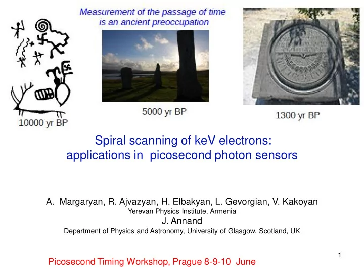
Spiral scanning of keV electrons: applications in picosecond photon sensors
- A. Margaryan, R. Ajvazyan, H. Elbakyan, L. Gevorgian, V. Kakoyan
Yerevan Physics Institute, Armenia
- J. Annand
Department of Physics and Astronomy, University of Glasgow, Scotland, UK
Picosecond Timing Workshop, Prague 8-9-10 June