Paper Review 
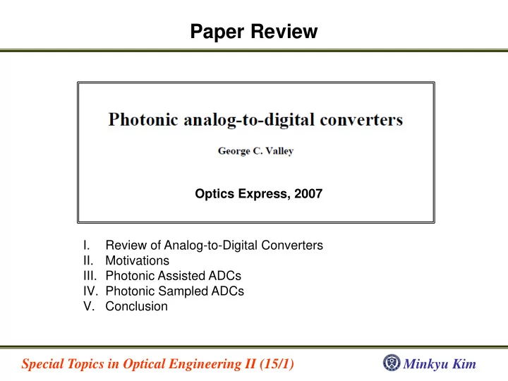
Optics Express, 2007 I. Review of Analog-to-Digital Converters II. Motivations III. Photonic Assisted ADCs IV. Photonic Sampled ADCs V. Conclusion Special Topics in Optical Engineering II (15/1) Minkyu Kim
Analog-to-Digital Converter β’ Analog-to-digital converter -Sampling(S/H or T/H) + Quantization(Quantizer) -Sampling frequency, resolution(N bits) are important specs ex)6-bit 500MS/sec ADC Special Topics in Optical Engineering II (15/1) Minkyu Kim
ADC Basics <Sampling & Quantization> <V in vs Digital Output & Quantization error> β’ SNR Calculation ππππΆ 2 1 2 ππ = π 3 2 2 2π -Quantization error energy = 2 π πππΆ π πππΆ -SNR(Signal-to-Noise Ratio) = ππ£π’ ππππΆ 12 β 2 ο¨ SNR(dB) = 1.76 + π Γ 6.02 π’=π π΅π‘ππ 2 ππ’ ππ’ = π΅ 2 2 2π π 2 1 -Signal energy = 2 = πππΆ π ο¨ N = [SNR(dB)-1.76]/6.02 π’=0 8 Special Topics in Optical Engineering II (15/1) Minkyu Kim
Resolution Degradation <Actual quantization with noise and nonlinearities> β’ Factors inducing resolution degradation (1) Timing errors : random jitter, broadening of the sampling time (2) Amplitude errors : Random noise, nonlinearities β’ ENOB(Effective Number Of Bits) -Effective resolution from N -ENOB = [SINAD(dB) β 1.76]/6.02, SINAD(SIgnal-to-Noise And Distortion) Special Topics in Optical Engineering II (15/1) Minkyu Kim
Motivation for Photonic ADCs <State-of-art in electronic ADCs> Limited by many factors(Thermal noise, jitter, etc) ο¨ Photonic ADC push performance to limitations Special Topics in Optical Engineering II (15/1) Minkyu Kim
Classes of Photonic ADCs β’ Photonic Assisted ADCs -Electronic ADCs that use photonics to improve limiting properties β’ Photonic Sampled ADCs -Only sampling is performed in the optical domain β’ Photonic Quantized ADCs -Only quantization is performed in the optical domain β’ Photonic Sampled & Quantized ADCs -Both sampling & quantization is performed in optical domain Special Topics in Optical Engineering II (15/1) Minkyu Kim
Optical Link & Photonic ADCs <Generic analog optical link> β’ β’ CNR(Carrier-to-Noise Ratio) SFDR(Spur-Free Dynamic Range) πππ 2 /2 -Nonlinearities in an analog optical link - π·ππ = 2 +π ππ½π 2 2 +π π’β (π π‘ ) -Caused by both optical devices and RF -CNR is used in place of SNR in analog link spectrum - πΉπππΆ = π·ππ ππΆ β 1.76 /6.02 -No general formulation for arbitrary input spectra π βΆ ππππ£πππ’πππ ππππ’β π βΆ πππ‘ππππ‘ππ€ππ’π§ ππ ππΈ π βΆ πππ’ππππ πππ₯ππ π π‘ : πβππ’ ππππ‘π π π’β : πβππ πππ ππππ‘π π ππ½π : ππ½π ππππ‘π Special Topics in Optical Engineering II (15/1) Minkyu Kim
Optical Link & Photonic ADCs Assume RIN = 0, no path loss, linear <ENOB as a function of link BW for an analog optical link> High optical power is required for high resolution(>10 ENOB) ο¨ Moderate resolution & 10s of bandwidth ADC may be a better target for photonic ADCs Special Topics in Optical Engineering II (15/1) Minkyu Kim
Photonic Assisted ADCs Modes of cavity Periodic impulse train I. Sample using mode-locked laser FFT Ξ Ο Ξ T Ο t Γ β Gain curve Short pulse <General schematic of photonic assisted ADC> β’ Advantages -Faster rise time and lower pulse-to-pulse jitter Ο t = = -Can remove clock from ADC circuit with fiber -Address multiple points from one optical source Mode locked source Short pulse train β’ Disadvantages Ξ T - Integrating mode locked laser into commercial product is hard Ο t Special Topics in Optical Engineering II (15/1) Minkyu Kim
Photonic Assisted ADCs II. Optical track & hold -Limitation of direct illumination of a single optoelectronic switch (1) Capacitor is charged by weak input signal(Track) (2) Semiconductor lifetime is not enough short(Hold) a. Diode bridge β’ No optical pulse : diode bridge works(Track) β’ Optical pulse : diode bridge off(Hold) β’ Advantages -Reduced aperture time -Low clock jitter -Clock isolation ο¨ No clock/signal interference β’ 1 GS/s, 9.6 SNR bits achieved <Photonic assisted ADC using diode bridge circuit> Special Topics in Optical Engineering II (15/1) Minkyu Kim
Photonic Assisted ADCs II. Optical track & hold b. Photonic-assisted time-interleaved ADC <Electronic time-interleaved ADC> <Photonic assisted time-interleaved ADC> <Optically triggered differential S/H circuit> β’ 4 ENOB for input bandwidth up to 40 GHz achieved ο¨ approximately 6 times bandwidth of electronic ADCs Special Topics in Optical Engineering II (15/1) Minkyu Kim
Photonic Assisted ADCs III. Optically triggered electron beam ADC <Basic cathode ray tube ADC> <Optically triggered e-beam ADC> β’ Using mode-locked laser ο¨ low-jitter high repetition rate train of light pulse β’ ~4 ENOB for input bandwidth up to 100 GS/s achieved Special Topics in Optical Engineering II (15/1) Minkyu Kim
Photonic Sampled ADCs I. Photonic sampled ADC without DeMUX <Photonic sampled and electronically quantized ADC> β’ All of the timing characteristics are controlled by the low-noise optical clock β’ Sampling time is set by the pulse width, the bandwidth of modulator β’ Timing jitter is set by jitter of the laser β’ Several issues exist -Modulator linearity -PD responsivity -PD recovery time ο¨ DeMUX data Special Topics in Optical Engineering II (15/1) Minkyu Kim
Photonic Sampled ADCs II. Photonic sampled and demultiplexed ADC <Photonic sampled and demultiplexed ADC> β’ Achieved 505MS/s, ENOB = 9.8 β’ Two major sources of error : pulse-to-pulse amplitude fluctuation, timing jitter β’ Path matching is hard, calibration is needed Special Topics in Optical Engineering II (15/1) Minkyu Kim
Conclusion β’ Review of electronic ADCs β’ Overcome limitation of electronic ADCs with photonic ADCs β’ Photonic assisted ADCs β’ Photonic sampled ADCs Special Topics in Optical Engineering II (15/1) Minkyu Kim
Recommend
More recommend