Grating structures for novel applications
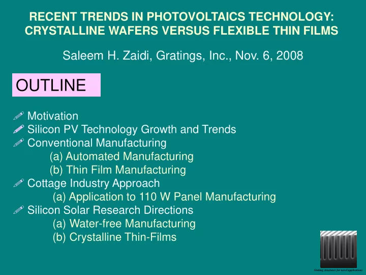
OUTLINE Motivation Silicon PV Technology Growth and Trends - - PowerPoint PPT Presentation
RECENT TRENDS IN PHOTOVOLTAICS TECHNOLOGY: CRYSTALLINE WAFERS VERSUS FLEXIBLE THIN FILMS Saleem H. Zaidi, Gratings, Inc., Nov. 6, 2008 OUTLINE Motivation Silicon PV Technology Growth and Trends Conventional Manufacturing (a)
Grating structures for novel applications
ACKNOWLEDGEMENTS
Sam McCormack, Richard Marquardt, Matt Channon, Robert Ellis, Karen DeZetter, Laure Koltunski, David Modisette, Rich Winder, Rajiv Prinja, Abdul Latif, Gary Begay, Bernard Stuart, Dr. J. Tringe, and Prof. K. Sopian
- Prof. S. Brueck, Dr. James Lyke, James Gee, Dr. D.
Ruby, John Wohlgemuth, and Steve Rockholm NSF, DoD, Sandia National Labs, UKM, and AFRL BP Solar, Adventsolar, LMCO
Grating structures for novel applications
INTRODUCTION TO GRATINGS
Turn-key solar cell and module manufacturing systems Multi-vapor etching systems Pulsed laser annealing systems Solar cells and Modules Nanostructures
Grating structures for novel applications
INTRODUCTION TO GRATINGS
Si nanostructure Au nanospheres Laser-etched Thru Features 110 W Panel 6-inch diameter Solar Cell
Grating structures for novel applications
United States 3816 billion KWh Annually Pakistan 66 billion KWh Annually Tanzania 1 billion KWh Annually
GLOBAL ELECTRICITY GENERATION
USA Russia Africa Green Land China Australia
Grating structures for novel applications
ELECTRICITY GENERATION VS GDP
Higher energy usage leads to higher income Most of the world at much lower income Quality-of-life linked to energy usage
Grating structures for novel applications
ELECTRICITY GENERATION IN ASIA
India and China will generate most electricity Coal usage will lead to environment degradation Climate is globally linked
Grating structures for novel applications
PARADIGM SHIFT IN ELECTRICITY GENERATION
Access to electricity is fundamental human right and responsibility Energy generation must be at the point of use Transition from macro grids (hundreds of miles) to nano grids (~ mile) Power plants from ~ 100s MW capacity to ~ 1 MW capacity Renewable PV technology to by-pass carbon-based fuels
FUNDAMENTAL ASSUMPTIONS
Grating structures for novel applications
COTTAGE INDUSTRY APPROACH TO PHOTOVOLTAICS
A solar cell is just a large area diode Manufacturing model based on IC model is not needed Energy conversion costs ($/W) is the key parameter PV technology is adaptable to a society’s technological level Investment in PV technology infrastructure (education, economy) PV technology creates jobs FUNDAMENTAL ASSUMPTIONS
Grating structures for novel applications
PV RESIDENTIAL APPLICATIONS
BIPV ~ 2-5 kW
Grating structures for novel applications
PV INDUSTRIAL APPLICATIONS
Industrial ~ 0.1-1 M W Agriculture ~ 0.1-1 kW Power Plant ~ 1 M W
Grating structures for novel applications
PV Power in MW PV Power in MW
Cumulative PV Power From 1990-2005 PV Power From 2001-2005
PV INDUSTRY OVERVIEW
Sustained Growth over Last 15 Years Grid-integrated PV is dominant Off-grid is economically profitable today!
Grating structures for novel applications
PV GENERATION SECTORS IN USA
Grid-connected ~ 90 % of the Total Significant residential and commercial sectors Off-grid growth is ~ 10 % of total
2005 installations ~ 100 MW
Grating structures for novel applications
IMPACT OF SUBSIDIES ON PV GENERATION
Residential Programs in Japan
PV Growth is dependent on subsidies Costs in Grid-connected regions still too high Off-grid regions, PV is the most economical
Grating structures for novel applications
PV GENERATION BY TECHNOLOGY SECTORS
Multicrystalline Si is Dominant Monocrystalline Si share has increased Thin-film technologies have reduced
Grating structures for novel applications
3.25 GW Generation 4 GW Generation
PROJECTED PV GROWTH IN NEXT FEW YEARS
Germany and Japan will lead growth China will compete strongly ROW and US may lag behind
Grating structures for novel applications
PV INDUSTRY OUTLOOK --- Wall Street Analysis
- Huge financial growth in 2003 to 2008 with competing
technologies Period of consolidation 2009 through 2012 Financial activity will rebound, partly from merger and acquisition Grid-Parity ~ 2015
Grating structures for novel applications
PRINCIPAL PV TECHNOLOGY SECTORS
Raw material to purified Si Mono/poly silicon wafers from feedstock Wafer processing into solar cells Solar cell packaging into modules Module arrays for system integration
Grating structures for novel applications
PV TECHNOLOGY SECTOR: SILICON PURIFICATION
Si is the 2nd most abundant element on earth; Si is ~ 25.7 % of Earth’s mass Si is capable of supplying all our Energy
Raw SiO2 produced by Mining Purified Silicon Feedstock
Grating structures for novel applications
SUMMARY 2005
Hemlock 7,700 Wacker Polysilicon 5,600 REC 5,550 Tokuyama 5,200 MEMC 3,800 Mitsubishi Materials 1,600 Mitsubishi Polysilicon 1,260 Sumitomo Titanium 700 Other 220 TOTAL 31,630
Very expensive to produce purified Si Dominated by few companies Production of feedstock in tonnes annually
MAJOR PRODUCERS OF PURIFIED SILICON
Grating structures for novel applications
PV TECHNOLOGY SECTOR: MONOCRYSTALLINE AND POLYCRYSTALLINE SILICON MANUFACTURING
Cast Growth Poly-Si CZ-Growth Mono-Si Critical Technology Wafer manufacturing: key to success Mono-Si superior to and more expensive than Poly-Si Gratings focus on mono-Si
Grating structures for novel applications
BRIEF INTRO TO SILICON SOLAR CELL
Converts sunlight into electricity Silicon Wafer is processed into solar cell Current Extraction uses Screen Printing and Electroplating Optical Absorption in thinner wafers using 3D Structures Cell Efficiencies ~ 10-20 % range
Solar Spectrum on Earth Basic Cell Configuration
Grating structures for novel applications
PRINCIPAL SOLAR CELL MANUFACTURING STEPS
Damage Removal
NOTES: Technology Trend: Thinner Wafers and Dry Processing Need for Low-Thermal Budget Processes Replacement of Screen-Printing by Electroplating High throughput using Automated Equipment
Grating structures for novel applications
LARGE VOLUME, HIGH COST MANUFACTURING APPROACH USING TURNKEY SYSTEMS Following IC manufacturing model High throughput to meet profitability
Automated Acid Etch System
Grating structures for novel applications
LARGE VOLUME, HIGH COST MANUFACTURING APPROACH USING TURNKEY SYSTEMS
Automated Diffusion System
Several approaches are used POCl3 produces best results
Grating structures for novel applications
LARGE VOLUME, HIGH COST MANUFACTURING APPROACH USING TURNKEY SYSTEMS
Automated Edge Isolation System Automated Nitride System
Several process approaches Proprietary and commercial systems PECVD nitride is often the most expensive machine
Grating structures for novel applications
LARGE VOLUME, HIGH COST MANUFACTURING APPROACH USING TURNKEY SYSTEMS
Screen Printing System Contact Firing System
Low-cost screen printing options available Contact firing system is unique to screen printing
Grating structures for novel applications
LARGE VOLUME, HIGH COST MANUFACTURING APPROACH USING TURNKEY SYSTEMS
Automated Solar Cell Tester
High Throughput Robotics for Cell Transfer and Sorting
Grating structures for novel applications
SOLAR CELL MANUFACTURING CHALLENGES High wafer cost relative to conventional fuels Wafer supplies for smaller companies High wafer costs High startup costs in extensive automation Harmful Chemicals Extensive water usage Lack of Innovation due to cost considerations
Grating structures for novel applications
THIN-FILM CIGS MANUFACTURING PROCESS
Large area vacuum equipment High power lasers
Grating structures for novel applications
TYPICAL CIGS PRODUCTION LINE Startup costs ~ US $ 30 million Annual production ~ 10 MW/year
Grating structures for novel applications
RETURN ON INVESTMENT PROJECTIONS High profitability High initial investment
Grating structures for novel applications
LOW COST MANUFACTURING PROCESS Modular approach Step-wise process characterization Efficiency ~ 15-18 % range
Grating structures for novel applications
SURFACE TEXTURING FOR PERFORMANCE ENHANCEMENT
RIE Texture Wet-Chemical Texture Spectral Reflectance
Cell Description Eff. (%) Open Circuit Voltage (V) Short Circuit Current (A) Fill Factor
Planar 14.5 0.611 1.269 0.786 RIE 16.48 0.617 1.434 0.781 chemical 16.96 0.619 1.452 0.792
Grating structures for novel applications
LOW VOLUME, LOW COST MANUFACTURING APPROACH PRINCIPAL PROCESSES and EQUIPMENT
LabVIEW Interface Coin stack Wafer Arrangement Etching Gas from Sidewalls 6”-diameter wafer capability
Gratings Edge Isolation System
Grating structures for novel applications
LOW VOLUME, LOW COST MANUFACTURING APPROACH PRINCIPAL PROCESSES and EQUIPMENT
Manual Solar Cell Tester
LabVIEW Interface Cells and Modules Programmable Power Supply
Grating structures for novel applications
SCREEN-PRINTED, TEXTURED 6”-DIAMETER SOLAR CELLS
Cell Description Eff. (%) Open Circuit Voltage (V) Short Circuit Current (A) Fill Factor
Wet- chemical 15.686 0.605 6.407 0.725
Grating structures for novel applications
PRINCIPAL SOLAR MODULE MANUFACTURING STEPS
Technology Trend: High throughput using Automated Equipment Combine Cell and Module Manufacturing Operations Opportunities for low-cost, Manual Manufacturing NOTES:
Grating structures for novel applications
LARGE VOLUME, HIGH COST MANUFACTURING APPROACH USING TURNKEY SYSTEMS
Automated Solar Cell Tester and Sorter
High Throughput Robotic for Cell Transfer and Sorting
Grating structures for novel applications
- LARGE VOLUME, HIGH COST MANUFACTURING
APPROACH USING TURNKEY SYSTEMS
Automated Solar Cell Tabbing and Soldering
Grating structures for novel applications
LARGE VOLUME, HIGH COST MANUFACTURING APPROACH USING TURNKEY SYSTEMS
Automated Lamination Module Tester
High Throughput at High Cost Robotic for Cell Transfer and Sorting
Grating structures for novel applications
LOW COST MANUFACTURING APPROACH PRINCIPAL PROCESSES and EQUIPMENT
Manual Cell Tabbing Manual Cell Stringing
Low cost and effective Employment oriented Simple throughput extension
Grating structures for novel applications
Manual Operation Light tables for defect detection Yields comparable to automated equipment
LOW COST MANUFACTURING APPROACH PRINCIPAL PROCESSES and EQUIPMENT
Grating structures for novel applications
LOW COST MANUFACTURING APPROACH
MODULE LAMINATION AND FRAMING
Manual operation Manual loading of laminator Manual Framing
Manual Laminator
Grating structures for novel applications
LOW COST MANUFACTURING APPROACH SOLAR MODULE LIV CHARACTERIZATION
Manual operation Manual loading of modules
Module LIV Tester
Grating structures for novel applications
Reduced startup cost and employment oriented
LOW VOLUME, LOW COST MANUFACTURING APPROACH BASIC FACTORY LAYOUT
Grating structures for novel applications
Cross-over point ~ 2 MW/year in US Cross-over point ~ 0.5 MW/year in developing country
COST AND BENEFIT ANALYSIS
Grating structures for novel applications
SILICON SOLAR RESEARCH DIRECTIONS
NEEDS FOR WATER-FREE MANUFACTURING
1 MW production requires ~ 10 million Gal DI water Harmful chemicals such as HF, HCl, NaOH Reduced yields for Thinner wafers Al BSF process incompatibility on Thinner wafers
PLASMA PROCESSES IN SOLAR CELL MANUFACTURING
Plasma texturing Plasma implantation Reduced thermal budget No wet-chemical processing
Grating structures for novel applications
PLASMA PROCESSES IN SOLAR CELL MANUFACTURING
IQE PLANAR
Wavelength (nm)
400 600 800 1000 1200
IQE and Reflectance
20 40 60 80 100
IQE--TEXTURED Ref--PLANAR Ref--PLANAR
Random RIE Texture Plasma implantation System Implant Profile Reflection and IQE
Grating structures for novel applications
SILICON SOLAR RESEARCH DIRECTIONS
NEED FOR CRYSTALLINE SILICON THIN-FILMS
Reduce energy conversion costs Flexible substrates Higher Efficiencies
THIN-FILM SOLAR CELL MANUFACTURING
Epitaxial growth Porous Si etching and de-lamination Reduced optical absorption Expensive and low throughput
Grating structures for novel applications
OPTICAL ABSORPTION IN THIN FILMS
Surface Texture Surface and Sidewall Texture Short-circuit Enhancement Short-circuit Enhancement
Grating structures for novel applications
OPTICAL ABSORPTION IN THIN FILMS
Short-circuit Enhancement Short-circuit Enhancement
Grating structures for novel applications
CONCLUDING THOUGHTS ON PV TECHNOLOGY
On-Grid PV Off-Grid Village-No Electricity PV Technology is Special Needed Most by Poorest of the Poor PV Technology is Expensive PV Technology Must Become Indigenous PV technology Must evolve Into Cottage/ Community Industry PV Technology Combines Silicon, Oxygen, And Sun---abundant and free
Grating structures for novel applications