
SLIDE 1
1
Introduction to CMOS VLSI Design
Lecture 2: MIPS Processor Example
David Harris
Harvey Mudd College Spring 2004
2: MIPS Processor Example Slide 2 CMOS VLSI Design
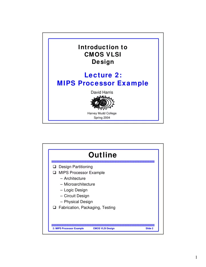
Outline Design Partitioning MIPS Processor Example Architecture - - PDF document
Introduction to CMOS VLSI Design Lecture 2: MIPS Processor Example David Harris Harvey Mudd College Spring 2004 Outline Design Partitioning MIPS Processor Example Architecture Microarchitecture Logic Design
Harvey Mudd College Spring 2004
2: MIPS Processor Example Slide 2 CMOS VLSI Design
2: MIPS Processor Example Slide 3 CMOS VLSI Design
2: MIPS Processor Example Slide 4 CMOS VLSI Design
2: MIPS Processor Example Slide 5 CMOS VLSI Design
2: MIPS Processor Example Slide 6 CMOS VLSI Design
2: MIPS Processor Example Slide 7 CMOS VLSI Design
2: MIPS Processor Example Slide 8 CMOS VLSI Design
2: MIPS Processor Example Slide 9 CMOS VLSI Design
2: MIPS Processor Example Slide 10 CMOS VLSI Design
2: MIPS Processor Example Slide 11 CMOS VLSI Design
format example encoding R I J ra rb rd funct
ra rb imm 6 6 6 6 5 5 5 5 5 5 16 26 add $rd, $ra, $rb beq $ra, $rb, imm j dest dest
2: MIPS Processor Example Slide 12 CMOS VLSI Design
2: MIPS Processor Example Slide 13 CMOS VLSI Design
2: MIPS Processor Example Slide 14 CMOS VLSI Design
2: MIPS Processor Example Slide 15 CMOS VLSI Design
format example encoding R I J ra rb rd funct
ra rb imm 6 6 6 6 5 5 5 5 5 5 16 26 add $rd, $ra, $rb beq $ra, $rb, imm j dest dest
2: MIPS Processor Example Slide 16 CMOS VLSI Design
2: MIPS Processor Example Slide 17 CMOS VLSI Design
PC M u x 1 Registers Write register Write data Read data 1 Read data 2 Read register 1 Read register 2 Instruction [15: 11] M u x 1 M u x 1 1 Instruction [7: 0] Instruction [25: 21] Instruction [20: 16] Instruction [15: 0] Instruction register ALU control ALU result ALU Zero Memory data register A B IorD MemRead MemWrite MemtoReg PCWriteCond PCWrite IRWrite[3:0] ALUOp ALUSrcB ALUSrcA RegDst PCSource RegWrite Control Outputs Op [5: 0] Instruction [31:26] Instruction [5: 0] M u x 2 Jump address Instruction [5: 0] 6 8 Shift left 2 1 1 M u x 3 2 M u x 1 ALUOut Memory MemData Write data Address PCEn ALUControl
2: MIPS Processor Example Slide 18 CMOS VLSI Design
PCWrite PCSource = 10 ALUSrcA = 1 ALUSrcB = 00 ALUOp = 01 PCWriteCond PCSource = 01 ALUSrcA =1 ALUSrcB = 00 ALUOp= 10 RegDst = 1 RegWrite MemtoReg = 0 MemWrite IorD = 1 MemRead IorD = 1 ALUSrcA = 1 ALUSrcB = 10 ALUOp = 00 RegDst=0 RegWrite MemtoReg =1 ALUSrcA = 0 ALUSrcB = 11 ALUOp = 00 MemRead ALUSrcA = 0 IorD = 0 IRWrite3 ALUSrcB = 01 ALUOp = 00 PCWrite PCSource = 00 Instruction fetch Instruction decode/ register fetch Jump completion Branch completion Execution Memory address computation Memory access Memory access R-type completion Write-back step ( O p = ' L B ' )
( O p = ' S B ' ) (Op = R-type) (Op = 'BEQ') (Op = 'J') (Op = 'S B') (Op = 'L B') 7 4 12 11 9 5 10 8 6 Reset MemRead ALUSrcA = 0 IorD = 0 IRWrite2 ALUSrcB = 01 ALUOp = 00 PCWrite PCSource = 00 1 MemRead ALUSrcA = 0 IorD = 0 IRWrite1 ALUSrcB = 01 ALUOp = 00 PCWrite PCSource = 00 2 MemRead ALUSrcA = 0 IorD = 0 IRWrite0 ALUSrcB = 01 ALUOp = 00 PCWrite PCSource = 00 3
2: MIPS Processor Example Slide 19 CMOS VLSI Design
reset ph1 ph2 crystal
2-phase clock generator MIPS processor adr writedata memdata external memory memread memwrite 8 8 8
2: MIPS Processor Example Slide 20 CMOS VLSI Design
datapath controller alucontrol
ph1 ph2 reset memdata[7:0] writedata[7:0] adr[7:0] memread memwrite
zero pcen regwrite irwrite[3:0] memtoreg iord pcsource[1:0] alusrcb[1:0] alusrca aluop[1:0] regdst funct[5:0] alucontrol[2:0]
PC M u x 1 Registers Write register Write data Read data 1 Read data 2 Read register 1 Read register 2 Instruction [15: 11] M u x 1 M u x 1 1 Instruction [7: 0] Instruction [25: 21] Instruction [20: 16] Instruction [15: 0] Instruction register ALU control ALU result ALU Zero Memory data register A B IorD MemRead MemWrite MemtoReg PCWriteCond PCWrite IRWrite[3:0] ALUOp ALUSrcB ALUSrcA RegDst PCSource RegWrite Control Outputs Op [5: 0] Instruction [31:26] Instruction [5: 0] M u x 2 Jump address Instruction [5: 0] 6 8 Shift left 2 1 1 M u x 3 2 M u x 1 ALUOut Memory MemData Write data Address PCEn ALUControl 2: MIPS Processor Example Slide 21 CMOS VLSI Design
mips controller alucontrol datapath standard cell library bitslice zipper alu and2 flop inv4x mux2 mux4 ramslice fulladder nand2 nor2
inv tri
2: MIPS Processor Example Slide 22 CMOS VLSI Design
2: MIPS Processor Example Slide 23 CMOS VLSI Design
module fulladder(input a, b, c,
sum s1(a, b, c, s); carry c1(a, b, c, cout); endmodule module carry(input a, b, c,
assign cout = (a&b) | (a&c) | (b&c); endmodule
a b c s cout carry sum s a b c cout fulladder
2: MIPS Processor Example Slide 24 CMOS VLSI Design
2: MIPS Processor Example Slide 25 CMOS VLSI Design
2: MIPS Processor Example Slide 26 CMOS VLSI Design
2: MIPS Processor Example Slide 27 CMOS VLSI Design
2: MIPS Processor Example Slide 28 CMOS VLSI Design
a b a c b c cout x y z g1 g2 g3 g4
2: MIPS Processor Example Slide 29 CMOS VLSI Design
a b c c a b b a a b cout cn n1 n2 n3 n4 n5 n6 p6 p5 p4 p3 p2 p1 i1 i3 i2 i4 module carry(input a, b, c,
wire i1, i2, i3, i4, cn; tranif1 n1(i1, 0, a); tranif1 n2(i1, 0, b); tranif1 n3(cn, i1, c); tranif1 n4(i2, 0, b); tranif1 n5(cn, i2, a); tranif0 p1(i3, 1, a); tranif0 p2(i3, 1, b); tranif0 p3(cn, i3, c); tranif0 p4(i4, 1, b); tranif0 p5(cn, i4, a); tranif1 n6(cout, 0, cn); tranif0 p6(cout, 1, cn); endmodule
2: MIPS Processor Example Slide 30 CMOS VLSI Design
.SUBCKT CARRY A B C COUT VDD GND MN1 I1 A GND GND NMOS W=1U L=0.18U AD=0.3P AS=0.5P MN2 I1 B GND GND NMOS W=1U L=0.18U AD=0.3P AS=0.5P MN3 CN C I1 GND NMOS W=1U L=0.18U AD=0.5P AS=0.5P MN4 I2 B GND GND NMOS W=1U L=0.18U AD=0.15P AS=0.5P MN5 CN A I2 GND NMOS W=1U L=0.18U AD=0.5P AS=0.15P MP1 I3 A VDD VDD PMOS W=2U L=0.18U AD=0.6P AS=1 P MP2 I3 B VDD VDD PMOS W=2U L=0.18U AD=0.6P AS=1P MP3 CN C I3 VDD PMOS W=2U L=0.18U AD=1P AS=1P MP4 I4 B VDD VDD PMOS W=2U L=0.18U AD=0.3P AS=1P MP5 CN A I4 VDD PMOS W=2U L=0.18U AD=1P AS=0.3P MN6 COUT CN GND GND NMOS W=2U L=0.18U AD=1P AS=1P MP6 COUT CN VDD VDD PMOS W=4U L=0.18U AD=2P AS=2P CI1 I1 GND 2FF CI3 I3 GND 3FF CA A GND 4FF CB B GND 4FF CC C GND 2FF CCN CN GND 4FF CCOUT COUT GND 2FF .ENDS
2: MIPS Processor Example Slide 31 CMOS VLSI Design
2: MIPS Processor Example Slide 32 CMOS VLSI Design
datapath 2700 λ x 1050 λ (2.8 Mλ2 ) alucontrol 200 λ x 100 λ (20 kλ2 ) zipper 2700 λ x 250 λ 2700 λ 1690 λ wiring channel: 30 tracks = 240 λ mips (4.6 Mλ2 ) bitslice 2700 λ x 100 λ control 1500 λ x 400 λ (0.6 Mλ2 ) 3500 λ 3500 λ 5000 λ 5000 λ 10 I/O pads 10 I/O pads 10 I/O pads 10 I/O pads
2: MIPS Processor Example Slide 33 CMOS VLSI Design
2: MIPS Processor Example Slide 34 CMOS VLSI Design
2: MIPS Processor Example Slide 35 CMOS VLSI Design
2: MIPS Processor Example Slide 36 CMOS VLSI Design
A A A A A A A A A A A A A A A A B B B B C C D
2: MIPS Processor Example Slide 37 CMOS VLSI Design
2: MIPS Processor Example Slide 38 CMOS VLSI Design
2: MIPS Processor Example Slide 39 CMOS VLSI Design
2: MIPS Processor Example Slide 40 CMOS VLSI Design
2: MIPS Processor Example Slide 41 CMOS VLSI Design
Specification Architecture Design Logic Design Circuit Design Physical Design = = = = Function Function Function Function Timing Power
2: MIPS Processor Example Slide 42 CMOS VLSI Design
2: MIPS Processor Example Slide 43 CMOS VLSI Design