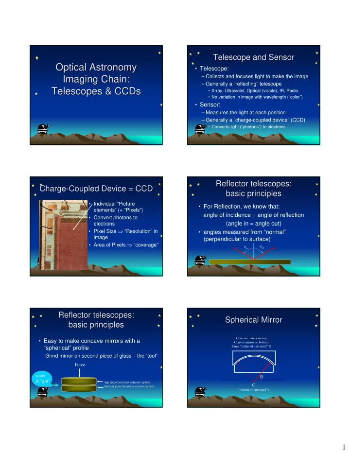
optical astronomy optical astronomy
play

Optical Astronomy Optical Astronomy Telescope: Collects and - PDF document

Telescope and Sensor Telescope and Sensor Optical Astronomy Optical Astronomy Telescope: Collects and focuses light to make the image Imaging Chain: Imaging Chain: Generally a reflecting telescope Telescopes & CCDs


  1. Telescope and Sensor Telescope and Sensor Optical Astronomy Optical Astronomy • Telescope: – Collects and focuses light to make the image Imaging Chain: Imaging Chain: – Generally a “reflecting” telescope Telescopes & CCDs Telescopes & CCDs • X-ray, Ultraviolet, Optical (visible), IR, Radio • No variation in image with wavelength (“color”) • Sensor: – Measures the light at each position – Generally a “charge-coupled device” (CCD) • Converts light (“photons”) to electrons Reflector telescopes: Reflector telescopes: Charge- -Coupled Device = CCD Coupled Device = CCD Charge basic principles basic principles • Individual “Picture • For Reflection, we know that: elements” (= “Pixels”) angle of incidence = angle of reflection • Convert photons to (angle in = angle out) electrons • Pixel Size ⇒ “Resolution” in • angles measured from “normal” image (perpendicular to surface) • Area of Pixels ⇒ “coverage” θ in θ out Reflector telescopes: Reflector telescopes: Spherical Mirror Spherical Mirror basic principles basic principles Concave mirror on top • Easy to make concave mirrors with a Convex mirror on bottom Same “radius of curvature” R “spherical” profile Grind mirror on second piece of glass – the “tool” Force water R & “grit” top piece becomes concave sphere C bottom piece becomes convex sphere (“center of curvature”) 1

  2. Concave Concave “ “Spherical Spherical” ” Mirror Mirror Correct Mirror Surface for Correct Mirror Surface for Works Poorly for Imaging Stars Works Poorly for Imaging Stars ∞ Object at ∞ Object at • Paraboloid! • Reflected rays from source at ∞ at – somewhat “shallower” curve than sphere different “heights” do not “focus” (cross • z = kx 2 for paraboloid optic axis) at same distance from mirror – parallel incident rays brought to common focus paraboloid sphere x z • This is called “Spherical Aberration!” – This is what plagued the Hubble Space Telescope Basic Designs of Optical Basic Designs of Optical F# (F- -ratio) and ratio) and “ “Plate Scale Plate Scale” ” F# (F Reflecting Telescopes Reflecting Telescopes f = F # • • “Prime focus” D – D = diameter – light is brought to focus by primary mirror only! • “Newtonian” – f = focal length – flat, diagonal secondary mirror deflects light out of tube – must consider focal length of combination of • “Cassegrain” primary & any secondary mirrors – convex secondary mirror reflects light through hole in primary • Determines “plate scale” • “Nasmyth” (or coudé) focus – angle increment of image per unit length at focal – tertiary mirror to redirect light to external instruments plane (e.g., arcsec per mm) S – “coudé” = “elbow” in French θ = – estimated from (our old friend): small-angle f θ relation 1 1 = = = plate scale ⋅ S f F # D Example of Plate Scale Example of Plate Scale θ 1 = = plate scale ⋅ S F # D Sensors with “ “Pixels Pixels” ” Sensors with • 10"-diameter f/16 telescope (different from “ (different from “emulsions emulsions” ”) ) 1 1 arcseconds = = ≅ × − 4 plate scale 2 . 5 10 ⋅ ⋅ F# D 16 254 mm mm 2

  3. Basic Concepts of CCD Sensors Basic Concepts of CCD Sensors CCDs: CCDs : “ “pixel scale pixel scale” ” • “Pixelated” ⇒ discrete picture elements • Example: (“pixels”) – assume plate scale of image = 50 arcsec per mm • Converts Photons to Electrons by – CCD pixel size (linear dimension) absorption and conversion of energy = 25 microns = 25 µ m = 0.025 mm = 25,000 nm • Sensitive over wide range of wavelengths arcseconds mm arcseconds = × = (“colors”) pixel scale 50 0 . 025 1 . 25 mm pixel pixel • Pixels are “read out” in sequence ⇒ pixel scale = 1.25 arcsec per pixel – cannot be randomly accessed!! CCDs: field of view CCDs : field of view CCDs: : “ “field of view field of view” ” CCDs • Want to match CCD pixel scale to image • Example: – CCD with 1,000,000 pixels (1 Mpixel) in 1000 × 1000 “blur” due to diffraction array • Recall main sources of image blur – Each pixel is 25 µ m × 25 µ m – angular resolution of telescope due to – Pixel size is 1.25 arcsec “diffraction limit” ⇒ field of view is: – random variations in atmosphere ⇒ time- 1000 pixels × 1.25 arcsec per pixel = 1250 arcsec varying movement ≅ 21 arcmin • Ideal pixel scale: 2 CCD pixels ≥ width of – could image most of Moon’s surface on this CCD through this telescope optical “blur” ⇒ Image field of view then limited by size of CCD (number of pixels) F CCD bi f ll i l i What is a CCD? What is a CCD? Basic Principles of CCD Imaging in Astronomy • “CCD” = “Charge-Coupled Device” • Invented in 1970s, originally for: – Memory devices – Arithmetic data processing (computer chips) • Usually made of Silicon (“Si”) ⇒ Has Same Light-Sensitive Properties as Silicon Light Meters Based on Slides by Simon Tulloch: available from http://www.ing.iac.es/~smt/CCD_Primer/CCD_Primer.htm 3

  4. Spectral Response (sensitivity) Spectral Response (sensitivity) CCDs in Astronomy CCDs in Astronomy of Typical CCD of Typical CCD • Light-Sensitive Properties applied to Imaging • Revolutionized Astronomical Imaging UV Visible Light IR – Improved Light-Gathering Power of Telescopes by nearly 100 × (5 magnitudes!!) Relative • 2005 Amateur w/ 15-cm (6") Telescope + CCD can get Response similar performance as 1960 Professional with 1-m (40") Telescope + Photography • Now Considered to be “Standard” Sensor in Astronomical Imaging 300 400 500 600 700 800 900 1000 – Special Arrangements with Observatory Necessary Incident Wavelength [nm] to use Photographic Plates or Film • Response is large in visible region, falls off for ultraviolet (UV) and infrared (IR) What is a CCD? What is a CCD? Film/Plates Still Useful!! Film/Plates Still Useful!! • Crystal Form of Matter (typically Si) • Large field of view • Converts “Light” to “Electronic Charge” • Cheap! – Pattern of Charge = “Image” 1. “Digitized” – Analog Measurements (“Voltages”) Converted to Integer Values at Pixels 2. “Digitized” Measurements Stored as Computer File Electron States in Si Si Crystal Crystal Electron States in Si Crystal Structure Crystal Structure Si • Available States in Crystal Arranged in Discrete “Bands” of Energies • Regular Pattern of Si – Lower Band ≡ Valence Band atoms • More electrons – Fixed Separations – Upper Band ≡ Conduction Band • Atomic Structure Pattern “Perturbs” • Fewer electrons Electron Orbitals • No States Exist in “Gap” Between Bands – Changes Layout of Conduction Band of Electron States Available Electron - Increasing States “Gap” ≈ 1.26 electron-volts energy “Gap” (eV) - - - http://www.webelements.com/webelements/elements/text/Si/xtal.html Valence Band of Electron States 4

  5. Action of Light on Electron States Action of Light on Electron States Action of “ “Charge Carriers Charge Carriers” ” Action of • Carriers are “Free” to Move in the • Incoming Photon with Energy ≥ 1.26 eV Corresponding Band – Excites Electrons From “Valence Band” to – Electron e - moves in Conduction Band “Conduction Band” – Hole h + moves in Valence Band • Electron in Conduction Band Moves in the • Charge Carriers may be “Counted” Crystal “Lattice” Electronically • Excited Electron e - leaves “Hole” (“Lack of Electron” = h + ) in Valence Band – Measure the Number of Absorbed Electrons ≈ Number of Absorbed Photons – Hole = “Carrier” of Positive Charge λ corresponding to Wavelength λ Wavelength corresponding to Energy and Wavelength Energy and Wavelength E = 1.26 electron Volts E = 1.26 electron Volts • If Incident Wavelength λ > 1 µ m, Photon • 1 eV = 1.602 × 10 -12 erg = 1.602 × 10 -12 Joule CANNOT be Absorbed! ( ) ⎛ ⎞ m − × − ⋅ × 27 8 6.624 10 erg sec ⎜ 3 10 sec ⎟ – Insufficient Energy to “Kick” Electron to ⎝ ⎠ hc λ = = Conduction Band ⎛ ⎞ E erg × × − ⎜ 12 ⎟ 1.26 eV 1.602 10 ⎝ ⎠ eV ⇒ Silicon is “Transparent” to long λ = × − = 7 9.84 10 m 984 nm ⇒ CCDs constructed from Silicon are Not ⇒ To Energize Electron in Si Lattice Requires Sensitive to Long Wavelengths λ < 984 nm ≅ 1 µ m After Electron is Excited into After Electron is Excited into Generation of CCD Carriers Generation of CCD Carriers Conduction Band… …. . Conduction Band • Electron and Hole Usually “Recombine” Quickly – Charge Carriers are “Lost” photon photon • Prevent by Applying External Electric Field to “Separate” Electrons from Holes • Field Attracts “Sweeps” Electrons and Holes in Opposite Conduction Band Hole Directions: Electron – Field “Sweeps” Electrons and Holes Apart ⇒ They don’t recombine Valence Band • Maintains Population of Charge Carriers – Allows Carriers to be “Counted” 5

Download Presentation
Download Policy: The content available on the website is offered to you 'AS IS' for your personal information and use only. It cannot be commercialized, licensed, or distributed on other websites without prior consent from the author. To download a presentation, simply click this link. If you encounter any difficulties during the download process, it's possible that the publisher has removed the file from their server.

Recommend


More recommend