
7b.1
EE 457 Unit 7b
Main Memory Organization
7b.2
Motivation
- Organize main memory to
– Facilitate byte-addressability while maintaining… – Efficient fetching of the words in a cache block
- __________________________ helps us achieve this
7b.3
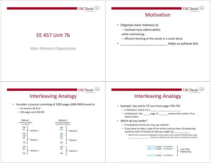
Interleaving Analogy
- Consider a journal consisting of 1000 pages (000-999) bound in
– 10 volumes (0-9) of – 100 pages each (00-99)
Method I
(Consecutive pages in a volume)
Method II
(Consecutive pages in consecutive volumes)
000 001 … 099 100 101 … 199 … 900 901 … 999 000 010 … 990 001 011 … 991 … 009 019 … 999
Volume 0 Volume 1 Volume 9 Volume 0 Volume 1 Volume 9
7b.4
Interleaving Analogy
- Example: Say article 73 runs from page 730-739
– In Method I: Article 73 is _______________________ – In Method II: The _____ page of _______ volume form article 73 as shown below
- Which do you prefer?
– If reading the article you may say method I – If you have to make a copy of the article and you have 10 photocopy machines with 10 friends to help you might say ____________
- Back to the scenario of reading the article, given those same 10 friends they could
_____________________ for you so that you can still read in a continuous manner
Page 730 is page 73 of volume 0 Page 731 is page 73 of volume 1 … Page 739 is page 73 of volume 9
Low Order Interleaving