
SLIDE 1
MESA+ INSTITUTE BRIDGING DISCIPLINES TO REALIZE NANO ENABLED - - PowerPoint PPT Presentation
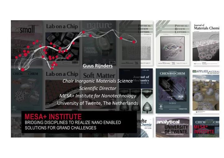
Guus Rijnders Chair Inorganic Materials Science Scientific Director MESA+ Institute for Nanotechnology University of Twente, The Netherlands MESA+ INSTITUTE BRIDGING DISCIPLINES TO REALIZE NANO ENABLED SOLUTIONS FOR GRAND CHALLENGES
Innovation
MESA+ Nanolab High Tech Factory
Darwin on a chip - MESA+ Institute together with CTIT Institute have demonstrated working electronic circuits that have been produced in a radically new way, using methods that resemble Darwinian evolution. The size of these circuits is comparable to the size of their conventional counterparts, but they are much closer to natural networks like the human brain.
World's most narrowband diode laser on a chip - MESA+ in collaboration with Lionix Company developed the world’s most narrowband diode laser on a chip exhibiting a quantum limited spectral bandwidth of less than 300 Hz. This laser concept represents a breakthrough in the fast-growing field of photonics, and will bring applications such as 5G internet and accurate GPS closer.
e-Nose - A fast and inexpensive breath test for early detection of diseases such as asthma and lung
As one of the few in the world, we have both the expertise and the technology to build such a sensitive device. Guus Rijnders: 'My goal is to use my expertise in nano-electronic materials to make people better or prevent people from becoming seriously ill'
Urine test for various types of cancer - Detecting cancer of various types, in a very early stage and using a simple urine sample. Research by University of Twente and the VU University Medical Center Amsterdam led to a new approach using nanotechnology. Together with a new startup company NanoMed Diagnostics, our researchers will further develop this towards a test that is ready for clinical use.
Highlights NanoNextNL programme
1 2 3 4 5 6 7 8 9
Basic Principle Observed Technology Concept Formulated Exp Proof of Concept Technology Validation in lab Technology Validation Relevant Environment Demo in Relevant Environment Demo in Operational Environment System Complete and Qualified Successful Mission Operations
………
Exploit the wide range of physical properties available in (complex) oxide materials Mixed oxides or Solid solutions Layered structures Superlattices Artificial constructed materials
STEM: SrTiO3-(La,Sr)MnO3
TEM: Superconducting superlattice, BaCuO-SrCuO
STEM: SrTiO3-LaAlO3
Liao, Z., et al, GR, Nature materials. 10.1038/NMAT4579
GR, D.H.A. Blank, “Build your own superlattice”, Nature 433 (2005) 369-370
Cubic LaAlO3 : 3.780 Å SrTiO3 : 3.905 Å SrRuO3 : 3.93 Å PbTiO3 : 3.90Å
SrMnO3 La0.5Sr0.5MnO3
Epitaxial growth: Temp.: 500-950 oC PO2: 10-6 – 100 mbar
Pulsed Laser Deposition with high-pressure RHEED
SrTiO3: surfaces with vicinal unit-cell steps with atomically flat terraces 250 nm single TiO2 termination
Koster et al. Appl. Phys. Lett 73 (1998) 2920 Kawasaki et al. Science 226 (1994) 1540
Single terminated perovskite substrates
single SrO termination Deposition of one unit cell of SrO
26 pulses at 10 Hz (4 Pa O2, 780 oC) 500 nm
Laser pulse Deposition pulse Supersaturation ~ 0.1 – 2 sec.
This enables measurement of the kinetic parameters at growth conditions by monitoring the decay of the adatom density between the deposition pulses.
PLD kinetics
RHEED intensity during homoepitaxial SrTiO3 growth
layer-by-layer growth
Fast deposition during one pulse.
Unit cell layer-by-layer SrTiO3 growth
Exploit the wide range of physical properties available in (complex) oxide materials Mixed oxides or Solid solutions Layered structures Superlattices Artificial constructed materials
NdGaO3-SrTiO3-(La,Sr)MnO3
TEM: Superconducting superlattice, BaCuO-SrCuO LSMO NG O STO LSM O NG O
STO
1 nm
LaAlO3-SrTiO3 interface Liao, Z., et al, GR, Nature materials. 10.1038/NMAT4579
GR, D.H.A. Blank, “Build your own superlattice”, Nature 433 (2005) 369-370
(a)-(b) Fabrication process of epitaxial PZT thin-film capacitors using PLD on SOI wafers (c) and (d) Schematic illustration of the surface micromachining process.
Understanding: functional properties of Pb(Zr,Ti)O3 films
BioMEMS pMUT Energy scavengers Inkjet
Breakdown voltage 𝑺𝒑𝒐 = 𝑀 𝑓𝑜𝑋𝝂
Usually, a buffer layer to reduce lattice mismatch is required to get high quality PZT.
Ga N B O A GaN a=3.19Å PZT a[110]=2.86Å PZT [111] GaN [0001] 10% mismatch Oxide/non-oxide Ga N O B Mg O A MgO a[110]=2.98Å MgO [111] 7% mismatch 4% mismatch O A B
Perovskite
Mg O
Face-center cubic Hexagonal
1.67 um 3 um MgO MgO 3 um
20 30 40 50 60 70 80 90
Intensity 2 Theta
12s
PZT (111)
Si GaN Si GaN
PZT (222) PZT
60 120 180 240
Intensity Phi
GaN MgO PZT
FWHM: 0.23 degree FWHM: 0.54 degree
2 4 6 8 10 12 14 120 0.0 0.2 0.4 0.6 0.8 1.0 1.2 1.4 1.6 1.8 2.0 2.2 2.4
FWHM MgO Thickness (nm)
(without MgO)
24.8nm Al0.2Ga0.8N GaN 3 nm MgO = 12 atomic planes PZT PZT
Al0.2Ga0.8N GaN
5 Å
19 in-plane lattice periods
200
20 40 60
Polarization (uC/cm2) Electric field (kV/cm)
0.24 nm 7 nm 78 nm
2 4 6 8 80 100 120 5 10 15 20 25 30 35
Pr (uC/cm 2) MgO thickness (nm)
2 4 6 8 80 100 120 5 10 15 20 25 30 35 40
Ec (KV/cm) MgO thickness (nm)
1 2 0.0 0.1 0.2 0.3 0.4 0.5 Ids(mA) Vgs(V)
Vds 2V
100 120 140 160 180 200 220 0.0 0.5 1.0 Ids(uA) Vdg(V/um)
1 2 3 4 5 0.0 0.1 0.2 0.3 0.4 Ids(mA) Vds(V)
Vg 0.25V Vg 0V Vg -0.25V Vg -0.5V Vg -0.75V Vg -1V Vg -1.25V Vg -1.5V Vg -1.75V Vg -2V
PZT
Al0.2Ga0.8N GaN