learning outcomes
play

Learning Outcomes I understand why a diode conducts current under - PowerPoint PPT Presentation

2-6.1 2-6.2 Learning Outcomes I understand why a diode conducts current under forward bias but does not under Spiral 2-6 reverse bias I understand the three modes of operation of a MOS transistor and the conditions Semiconductor


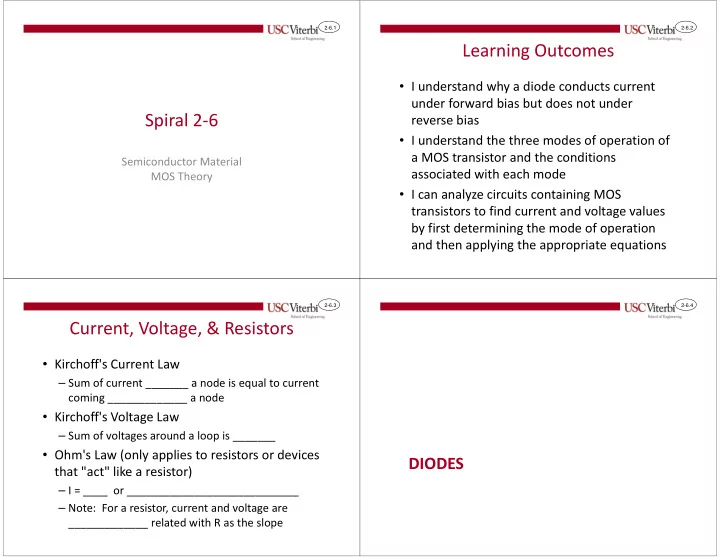
  1. 2-6.1 2-6.2 Learning Outcomes • I understand why a diode conducts current under forward bias but does not under Spiral 2-6 reverse bias • I understand the three modes of operation of a MOS transistor and the conditions Semiconductor Material associated with each mode MOS Theory • I can analyze circuits containing MOS transistors to find current and voltage values by first determining the mode of operation and then applying the appropriate equations 2-6.3 2-6.4 Current, Voltage, & Resistors • Kirchoff's Current Law – Sum of current _______ a node is equal to current coming _____________ a node • Kirchoff's Voltage Law – Sum of voltages around a loop is _______ • Ohm's Law (only applies to resistors or devices DIODES that "act" like a resistor) – I = ____ or ____________________________ – Note: For a resistor, current and voltage are _____________ related with R as the slope

  2. 2-6.5 2-6.6 Semiconductor Material Transistor Types p-type n-type p-type • Bipolar Junction Transistors (BJT) + + - – npn or pnp silicon structure • Semiconductor material is not a great conductor + – Small current into very thin base layer - + material in its pure form + controls large currents between emitter and + – Small amount of free charge collector emitter base collector – However the fact that it requires a current npn BJT • Can be implanted (“doped”) with other elements into the base means it burns power (P = I*V) (e.g. boron or arsenic) to be more conductive and thus limits how many we can integrate on a chip (i.e. density) Source Drain – Increases the amount of free charge Gate Input • Metal Oxide Semiconductor Field Effect + - - + - + + + + - Transistors conductive - + - - - - + polysilicon - + - - – nMOS and pMOS MOSFETS + - + - + - - - – Voltage applied to insulated gate controls + N-Type Silicon Pure Silicon P-Type Silicon + current between source and drain + (Doped with arsenic) (Doped with boron) n-type • Gate input requires no constant current…thus low p-type Electron donors Electron acceptors power! We will focus on MOSFET in this class N-type MOSFET 2-6.7 2-6.8 PN Junction Diode The PN Junction • Our understanding of how a transistor works will • When we join the two substances the free electrons at the junction will combine with the nearby free holes in a "loose" start by analyzing a simpler device: a diode bond • A diode can be formed by simply butting up some p- • This has two effects: type and n-type material together – Around the junction there are ______________ free charges (they've all combined) creating a _______________________ – Now remember the dopants in n- and p-type material are still _____________ charged (same # of protons/electrons). So this migration has actually created ions and thus an ________________ Cathode Anode + p-type n-type - (and thus voltage) in the opposite direction + - + + - p-type n-type + Schematic - + - - symbol of a diode + + - - Physical view

  3. 2-6.9 2-6.10 Depletion Region Forward Bias • Now let's place an external positive voltage source across the diode • Depletion region has __________ free or mobile charge – Holes and electrons are pushed toward each other and reduce the depletion region • A small ___________ is induced due to this recombination – If the external voltage is high enough the charges will have enough ________ – N-type material LOST an electron leaving a __________ ion to overcome the gap and start ______________ through the diode – P-Type material LOST a hole (GAINED an electron) leaving a – The positive external voltage needed to overcome the depletion region is ____________ ion known as the __________________ Voltage – The voltage is in the opposite direction V D + - - - - +++ - - - +++ + + n-type n-type p-type p-type + + - - - - + + + - + - p- n+ - - Human convention of Physical reality current as positive of electron flow charge flow Depletion Region Depletion Region 2-6.11 2-6.12 Ideal Diode Reverse Bias • A perfect diode would ideally allow current to flow in _______________________ • It would therefore be a perfect conductor in • Now let's place an external negative voltage source across the diode one direction (forward bias) and a perfect – Holes and electrons are attracted to the voltage source terminal (pulled away insulator in the other direction (reverse bias) from the depletion area making the depletion area expand) • Example: Determine the value of ID if a) VA = – ______ current is flowing across the junction because both holes and 5 volts (forward bias) and b) VD = -5 volts electrons are attracted in opposite directions (reverse bias) – Ideal model: -V D a) I D = _______ = __________ = 100 mA - + b) Diode is in reverse bias and is acting R S = 50 Ω like a perfect insulator, therefore no current can flow and I D = ______ I D - - - +++ – More realistic: + - p-type n-type + a) I D = _____________/R S = 86 mA + - V A + - b) I D = 0 _ + - Depletion Region

  4. 2-6.13 2-6.14 Carrier Concentration • Even silicon has some amount of free electrons (n) and holes (p) – We refer to this as the _________________________ concentration – Note: n = p since a free electron leaves a hole behind • When we add dopants we change the carrier concentration – N A and N D is the concentration of ____________ and _____________ respectively – Note: N A >> p and N D >> n TRANSISTORS + - - + - + + + + - - + - - - + - + - + - + - + - N-Type Silicon Pure Silicon P-Type Silicon (Doped with arsenic) (Doped with boron) Electron donors Electron acceptors 2-6.15 2-6.16 Doped Valence and Conduction Bands • Impurity atoms, i.e., donors or acceptors replace some silicon atoms in the crystal lattice – Donors: a valence of five e.g., phosphorus (P) or arsenic (As)) – Acceptors: a valence of three, e.g., boron (B)) – Remember these are electrically neutral (same # of protons/electrons), but are easily induced to donate or accept an electron under certain circumstances (i.e. under a voltage) • If the donors or acceptors get ionized, each donor delivers an A FEW QUICK NOTES electron to the conduction band. Also each acceptor will capture an electron from valence band leaving a hole behind – Normally, at room temperature all donors (density N D ) and acceptors (concentration N A ) are ionized 15

  5. 2-6.17 2-6.18 Conventions Body Terminal • Recall a PN junction acts like a diode and allows current flow when V pn > P N • Since the source is always at the lowest voltage (for NMOS) and V thresh highest voltage (for PMOS) we generally define all voltages w.r.t. • We don't want that current flow so we must always maintain appropriate voltage to keep the "intrinsic" diodes in _____________ V S – Always keep the P-type area at a voltage __________ than the N-type • Conventionally all terminal voltages are defined wrt V S • For NMOS: Keep Body = ______; For PMOS: Keep Body = ________ • We also often draw our schematic symbols w/o showing the body – We will often not show the body connection and assume it is appropriately connected terminal Gate Input Gate Input Source Input + Drain Output Drain Input - Source Input + - + n-type - p-type - + + - - + + - - + - + + + + + - - - - - + - + - - - - - + + -+ + + - + - + - + p-type n-type Body/Substrate Body/Substrate + + + + - - - - Vdd NMOS PMOS 18 2-6.19 2-6.20 Source or Drain • Since MOSFETs are symmetric, which terminal is the source and which is the drain? • It ____________________________! • For NMOS: Source is terminal connected to ________ voltage • For PMOS: Source is terminal connected to ________ voltage Gate Input Gate Input Source Input Source Input + Drain Output Drain Input - + - + n-type - p-type - + + - - + + - - + - + THE BASIC IDEA OF MOS + + + + - - - - - + - + - - - - - + + -+ + + - + - + - + OPERATION p-type n-type Body/Substrate Body/Substrate + + + + - - - - Vdd NMOS PMOS

Download Presentation
Download Policy: The content available on the website is offered to you 'AS IS' for your personal information and use only. It cannot be commercialized, licensed, or distributed on other websites without prior consent from the author. To download a presentation, simply click this link. If you encounter any difficulties during the download process, it's possible that the publisher has removed the file from their server.

Recommend


More recommend