SLIDE 1
Laser Based Assembly of Ultra Fine Pitch Bumped ICs For Chip-to-Chip Proximity Coupled Applications
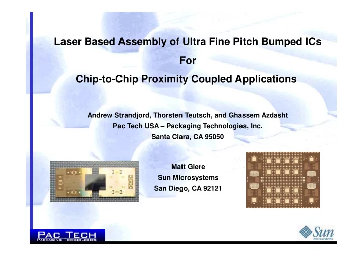
Andrew Strandjord, Thorsten Teutsch, and Ghassem Azdasht Pac Tech USA – Packaging Technologies, Inc. Pac Tech USA – Packaging Technologies, Inc. Santa Clara, CA 95050 Matt Giere Sun Microsystems San Diego, CA 92121
SLIDE 2
Flip Chip WLCSP Micro Bumps
50 100 150 200 250 350 µm
Solder Bumping Technologies (Bump Size)
Ultra Fine Pitch
Bump Size
BGA
300 50
Most Common Deposition Techniques: Paste Print, Electroplate, Sphere Drop, Sphere Transfer
SLIDE 3 Die-on-Die Memory-Stacking AC/DC - Coupled Stack Memory-on-DSP Passives-on-Die Memory-Stacks Ultra Fine Pitch Bumps for: High Density Interconnects (x-y) - Close Proximity Applications (y) High Speed RF Capacitive-Inductive
3D Integration ications
Backend/WLP- Solder FE/Fab - TSV - TCB Cu Backend/WLP- Solder
Samsung NC State
Chips and layout are different May require RDL DC current to all chips Close proximity Every chip the same
Applica Requirements Fab
StatChipPAC
SLIDE 4 Test Vehicle: 3 Chips ….. (2) Island – (1) Bridge Ultra Fine Pitch
Chip-to-Chip Proximity Coupled Test Vehicle Properties/Requirements:
µ µ µm)
µ µ µm)
- 8 inch wafers (Island & Bridge)
- Ceramic Substrate (w/cavity)
- Thinned Die (150 µ
µ µ µm)
Island Chip Island Chip 1 Island Chip 2 Substrate CSP Bumps Bridge Chip Pitch Bumps Proximity Coupled Interconnects Bridge Chip
SLIDE 5 Bridge Chip
Bridge Chip Ultra Fine Pitch Bond Pads
Specifications:
µ µ µm bond pads
Island Chip 1 Island Chip 2 Substrate Bridge Chip
Bridge Chip
X: 8680 m Y: 6520 m
Ultra Fine Pitch Bump Area
µ µ µm bond pads
µ µ µm passivation opening
µ µ µm pitch
µ µ µm resolution
µ µ µm chip-to-chip spacing
µ µ µm die thickness
SLIDE 6 Island Chip
Ultra Fine Pitch Bond Pads (30µ µ µ µm)
Island Chip
X: 15130 m Y: 12250 m Ultra Fine Pitch Bump Area (Overlap with Bridge Chip)
Island Chip 1 Island Chip 2 Substrate Bridge Chip
Specifications:
- 456 Bond Pads that match Bridge Chip
- 2856 Flip Chip Bumps (70µ
µ µ µm pads)
µ µ µm Bump Height
Flip Chip Bond Pads (70µ µ µ µm)
SLIDE 7 Three Chip Assembly
2 High Power Island Chips 1 Low Power Bridge Chip (<10W) Flip Chip Ultra Fine Pitch Bumping
+ +
Ceramic Substrate Laser Assembly Flip Chip Bumping Laser Assembly
Proximity Coupled Communication Low Power High Bandwidth Low Noise High Density Reference:
- M. Giere, et.al., “Proximity Communication
Flip-Chip Package with Micron Chip-to-chip Alignment Tolerances”, ECTC, Las Vegas, 2009.
SLIDE 8 Process Overview:
1) Deposit Ni/Au UBM (Bridge and Island) 3 µ µ µ µm 2) Bump Bridge Die (Sn) 2-3 µ µ µ µm Bump Island Die (SnPb) ~80 µ µ µ µm
Bridge Island
3) Thin & Dice Wafers 150 µ µ µ µm 4) Die Laser Assembly (1-Bridge to 2-Island) 5) Substrate Laser Assembly
Island Chip 1 Island Chip 2 Substrate Bridge Chip
SLIDE 9
e-Ni/Au Process on Aluminum: 1) Passivation Clean 2) Aluminum Etch 3) Zincation I 4) Zinc Strip 5) Zincation II 6) Electroless Nickel 7) Immersion Gold
e-Ni/Au UBM
Island & Bridge Island
Wafer Level Wet Chemical Batch: 50 w/hr
Plating
Batch: 50 w/hr
X
Plating Chemistry Control
PacLine-300 ™PacTech 3µm Ni 600Å Au
Zn II Zn II
Images are not to scale relative to each other 3µm Ni 600Å Au
SLIDE 10 Ni/Au Uniformity and Adhesion
1 2 3 4 5 6 7 8 9
Nickel/Gold uniformity across 8 inch wafer
1.5 1.7 1.9 2.1 2.3 2.5 2.7 2.9 3.1 3.3 3.5 1.5 1.7 1.9 2.1 2.3 2.5 2.7 2.9 3.1 3.3 3.5 1 2 3 4 5 6 7 8 9 10 Ni/Au Height above Al Pad (µ µ µ µm) Ni/Au Height above Passivaion (µ µ µ µm) Position On Wafer
Tall Nickel Average: 128.05 Max: 142.11 Min: 110.42 Std: 7.121 Mode: Al Fracture Shear Analysis 70 µm octagonal flip chip pads Tall Nickel
SLIDE 11
Double Layer Resist Process
Deposit Resist 1 Flood Expose Deposit Resist 2 Pattern Expose Develop & Descum
At IMAPS DPC 2009 reported 4 different technologies for lift off resist: 1) Three retro-resists 2) PMMA/Novolak stack After presentation, person from audience came up and suggested alternative 3) Use standard positive resist, coat twice, flood expose first layer, and
Ultra Fine Pitch Solder Bumping (Bridge Die)
Resist Develop & Descum Sputter Sn Strip Resists
expose first layer, and pattern expose second layer
3µm Sn LiftOff
SLIDE 12 Tin Sputtering
PE2400 Chilled Plate Slow Sputtering
1 2 3 4 5 6 7 8 9
Sn uniformity across 8 inch wafer
1.5 1.7 1.9 2.1 2.3 2.5 2.7 2.9 3.1 3.3 3.5 1 2 3 4 5 6 7 8 9 10 Sputtered Sn Height (µ µ µ µm) Position On Wafer
Smooth Sn on Liftoff Resist Wrinkled Sn on Liftoff Resist Sn Features on Bridge Die after Liftoff
SLIDE 13
Oven Reflow at 265-285ºC Flux and Oven Reflow Laser Reflow Vapor Phase Reflow 3µ µ µ µm Sn on NiAu (misaligned) 1) Nothing happens 2) Variable pull back 3) Black film
Wetability and Reflow Tests
(misaligned)
Elemental analysis shows Sn is highly oxidized Sputter thin Au layer on top of Sn (enabled by liftoff process) 500Å
SLIDE 14 Wetability and Reflow Tests
Oven Reflow w/Flux
completely onto the pads
converted to Sn- Ni intermetallics
completely onto the pads
=> Sn has not formed excessive IMC due to short pulse laser reflow
Pads Ni/Au and Sn/Au Laser Reflow No Flux
SLIDE 15 Flip Chip Solder Bumping (Island) 2856 bumps/die
Ultra SB2 ™PacTech
Capillary Reflow Laser
Production
SB2 ™PacTech
Prototyping
Requirements:
- High Yield Bumping Process
- Bump Uniformity
- Reliable Interconnect
- ~80 µm Bump Height (100 µm spheres)
- SnPb Eutectic
SLIDE 16 Flip Chip Bumped Die (SnPb Eutectic - 2856 bumps/die)
80 81 82 83 84 85 86 87 88 89 90 5 10 15 20 25 30 Bump Height above Passivaion (µ µ µ µm) Position On Wafer 1
Bump Height Ave: 84.93 σ: 0.78 3σ: 2.35
5 10 15 20 25 30 35 40 45 50 5 10 15 20 25 30 Shear Force (g) Position On Wafer 1
Shear Force
σ : 1.27 Cpk: 4.46 Failure Mode: Ductile Solder
SLIDE 17 Laser Assembly
1) Pickup Die & Align
( ±5 µm)
2) Contact
(10kgf)
3) Laser Reflow
LaPlace Assembly System™ PacTech
Placement accuracy: +/- 15um: 3000 - 5000 UPH
3) Laser Reflow
(20msec, Nd+3YAG)
Laser based assembly allows localized heating: • Selective to individual die
- Energy localized to bumped areas
- Ability to differentiate between solder alloys
- Low stress
- Minimizes IMC (time/temp)
Placement accuracy: +/- 15um: 3000 - 5000 UPH Placement accuracy: +/- 10um: ~2000 UPH Placement accuracy: +/- 5um: ~1000 UPH Placement accuracy: +/- 2.5um: ~500 UPH
3) SnPb 1) Sn 2) Sn 3) SnPb Mp SnPb = 183ºC Mp Sn = 232ºC
SLIDE 18 Assembly Process Steps:
- 1. Pick up Bridge Chip
- 2. Align Bridge Chip to first Island Chip
- 3. Bond Bridge Chip to first Island Chip by Laser Reflow
- 4. Pick up bonded Bridge-Island combination
- 5. Align Bridge-Island assembly to second Island Chip
Work In Progress
- 6. Bond Bridge-Island combination to the second Island
Chip by Laser Reflow
- 7. Pickup three chip assembly
- 8. Align to substrate
- 9. Bond Island-Bridge-Island combination to substrate
by Laser Reflow
SLIDE 19 Joint Integrity Tests
- No Shorts Observed
- No Opens Observed
- Good wetting on both
Bridge and Island after disassembly Bridge Die Island Die
SLIDE 20 Conclusions:
- Liftoff process versatile technique for creating ultra fine pitch Sn solder bump
- Au cap on Sn is essential for good wettability and reflow characteristics
- Laser reflow enables assembly of ultra fine pitch Sn bumps (minimizing IMC)
Ongoing Work:
- Variation in laser assembly energy, pulse width, contact force,…
Substrate cavity machining (Ceramic and Laminate)
- Substrate cavity machining (Ceramic and Laminate)
- FlipChip laser assembly to substrate
- Electrical & Capacitive signal transmission analysis
- Underfill studies
- Cross-section analysis of solder joints and intermetallics
- Variation in chip-to-chip spacing (e-Nickel thickness)