intel 8086
play

Intel 8086 Intel 8086 was launched in 1978. It was the first - PDF document

10/13/2010 Intel 8086 Intel 8086 was launched in 1978. It was the first 16-bit microprocessor. This microprocessor had major improvement over the execution speed of 8085. Gursharan Singh Tatla professorgstatla@gmail.com It is


  1. 10/13/2010 Intel 8086  Intel 8086 was launched in 1978.  It was the first 16-bit microprocessor.  This microprocessor had major improvement over the execution speed of 8085. Gursharan Singh Tatla professorgstatla@gmail.com  It is available as 40-pin Dual-Inline-Package (DIP). www.eazynotes.com www.eazynotes.com Gursharan Singh Tatla 1 Gursharan Singh Tatla 2 Intel 8086 Intel 8086  It has a 16 line data  It is available in three bus. versions:  And 20 line address  8086 (5 MHz) bus.  8086-2 (8 MHz)  It could address up to 1 MB of memory.  8086-1 (10 MHz)  It has more than  It consists of 29,000 20,000 instructions. transistors.  It supports multiplication and division. Gursharan Singh Tatla www.eazynotes.com Gursharan Singh Tatla www.eazynotes.com 3 4 
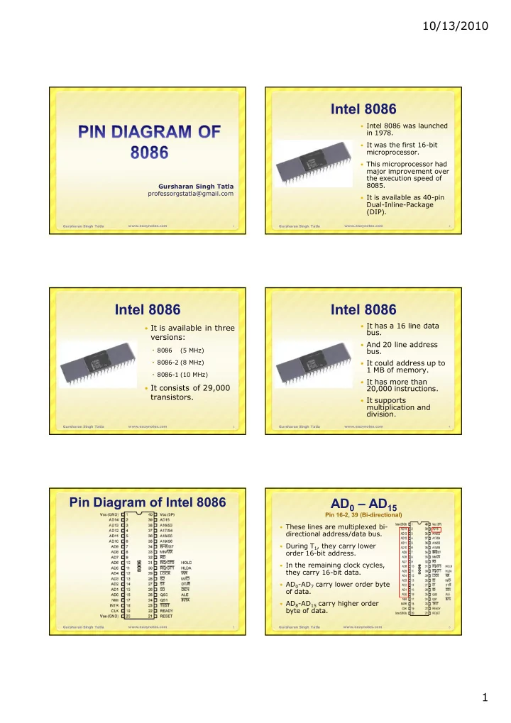
Pin Diagram of Intel 8086 AD 0 – AD 15 Pin 16-2, 39 (Bi-directional)  These lines are multiplexed bi- directional address/data bus.  During T 1 , they carry lower order 16-bit address.  In the remaining clock cycles, they carry 16-bit data.  AD 0 -AD 7 carry lower order byte of data.  AD 8 -AD 15 carry higher order byte of data. www.eazynotes.com www.eazynotes.com Gursharan Singh Tatla 5 Gursharan Singh Tatla 6 1

  2. 10/13/2010 A 19 /S 6 , A 18 /S 5 , A 17 /S 4 , A 16 /S 3 BHE / S 7 Pin 35-38 (Unidirectional) Pin 34 (Output)  BHE stands for Bus High  These lines are Enable. multiplexed unidirectional address and status bus.  BHE signal is used to indicate the transfer of data  During T 1 , they carry over higher order data bus higher order 4-bit address. (D 8 – D 15 ).  8-bit I/O devices use this  In the remaining clock signal. cycles, they carry status signals.  It is multiplexed with status pin S 7 . www.eazynotes.com www.eazynotes.com Gursharan Singh Tatla 7 Gursharan Singh Tatla 8 RD (Read) READY Pin 32 (Output) Pin 22 (Input)  This is an acknowledgement  It is a read signal used for signal from slower I/O read operation. devices or memory.  It is an output signal.  It is an active high signal.  It is an active low signal.  When high, it indicates that the device is ready to transfer data.  When low, then microprocessor is in wait state. Gursharan Singh Tatla www.eazynotes.com Gursharan Singh Tatla www.eazynotes.com 9 10 RESET INTR Pin 21 (Input) Pin 18 (Input)  It is a system reset.  It is an interrupt request signal.  It is an active high signal.  It is active high.  When high, microprocessor enters into  It is level triggered. reset state and terminates the current activity.  It must be active for at least four clock cycles to reset the microprocessor. www.eazynotes.com www.eazynotes.com Gursharan Singh Tatla 11 Gursharan Singh Tatla 12 2

  3. 10/13/2010 NMI TEST Pin 17 (Input) Pin 23 (Input)  It is a non-maskable  It is used to test the interrupt signal. status of math co- processor 8087.  It is an active high.  The BUSY pin of 8087 is  It is an edge triggered connected to this pin of interrupt. 8086.  If low, execution continues else microprocessor is in wait state. www.eazynotes.com www.eazynotes.com Gursharan Singh Tatla 13 Gursharan Singh Tatla 14 CLK V CC and V SS Pin 19 (Input) Pin 40 and Pin 20 (Input)  This clock input provides  V CC is power supply signal. the basic timing for  +5V DC is supplied processor operation. through this pin.  It is symmetric square  V SS is ground signal. wave with 33% duty cycle.  The range of frequency of different versions is 5 MHz, 8 MHz and 10 MHz. Gursharan Singh Tatla www.eazynotes.com Gursharan Singh Tatla www.eazynotes.com 15 16 MN / MX MN / MX Pin 33 (Input) Pin 33 (Input)  8086 works in two modes:  Pins 24 to 31 issue two different sets of signals.  Minimum Mode  One set of signals is issued  Maximum Mode when CPU operates in  If MN/MX is high, it works minimum mode. in minimum mode.  Other set of signals is  If MN/MX is low, it works issued when CPU operates in maximum mode. in maximum mode. www.eazynotes.com www.eazynotes.com Gursharan Singh Tatla 17 Gursharan Singh Tatla 18 3

  4. 10/13/2010 INTA Pin 24 (Output)  This is an interrupt Pin Description for acknowledge signal.  When microprocessor Minimum Mode receives INTR signal, it acknowledges the interrupt by generating this signal.  It is an active low signal. www.eazynotes.com www.eazynotes.com Gursharan Singh Tatla 19 Gursharan Singh Tatla 20 ALE DEN Pin 25 (Output) Pin 26 (Output)  This is an Address Latch  This is a Data Enable Enable signal. signal.  It indicates that valid  This signal is used to address is available on bus enable the transceiver AD 0 – AD 15 . 8286.  It is an active high signal  Transceiver is used to and remains high during T 1 separate the data from the state. address/data bus.  It is connected to enable pin  It is an active low signal. of latch 8282. Gursharan Singh Tatla www.eazynotes.com Gursharan Singh Tatla www.eazynotes.com 21 22 DT / R M / IO Pin 27 (Output) Pin 28 (Output)  This is a Data  This signal is issued by the Transmit/Receive signal. microprocessor to distinguish memory access  It decides the direction of from I/O access. data flow through the transceiver.  When it is high, memory is  When it is high, data is accessed. transmitted out.  When it is low, I/O devices  When it is low, data is are accessed. received in. www.eazynotes.com www.eazynotes.com Gursharan Singh Tatla 23 Gursharan Singh Tatla 24 4

  5. 10/13/2010 WR HLDA Pin 29 (Output) Pin 30 (Output)  It is a Write signal.  It is a Hold Acknowledge signal.  It is used to write data in memory or output device  It is issued after receiving depending on the status of the HOLD signal. M/IO signal.  It is an active high signal.  It is an active low signal. www.eazynotes.com www.eazynotes.com Gursharan Singh Tatla 25 Gursharan Singh Tatla 26 HOLD Pin 31 (Input)  When DMA controller Pin Description for needs to use address/data bus, it sends a request to Maximum Mode the CPU through this pin.  It is an active high signal.  When microprocessor receives HOLD signal, it issues HLDA signal to the DMA controller. Gursharan Singh Tatla www.eazynotes.com Gursharan Singh Tatla www.eazynotes.com 27 28 QS 1 and QS 0 S 0 , S 1 , S 2 Pin 24 and 25 (Output) Pin 26, 27, 28 (Output)  These status signals  These pins provide the indicate the operation status of instruction being done by the queue. microprocessor. QS 1 QS 0 Status  This information is 0 0 No operation required by the Bus 1 st byte of opcode from queue 0 1 Controller 8288. 1 0 Empty queue 1 1 Subsequent byte from queue  Bus controller 8288 generates all memory and I/O control signals. www.eazynotes.com www.eazynotes.com Gursharan Singh Tatla 29 Gursharan Singh Tatla 30 5

  6. 10/13/2010 S 0 , S 1 , S 2 LOCK Pin 26, 27, 28 (Output) Pin 29 (Output)  This signal indicates that S 2 S 1 S 0 Status other processors should not 0 0 0 Interrupt Acknowledge ask CPU to relinquish the system bus. 0 0 1 I/O Read 0 1 0 I/O Write  When it goes low, all 0 1 1 Halt interrupts are masked and 1 0 0 Opcode Fetch HOLD request is not 1 0 1 Memory Read granted. 1 1 0 Memory Write 1 1 1 Passive  This pin is activated by using LOCK prefix on any instruction. www.eazynotes.com www.eazynotes.com Gursharan Singh Tatla 31 Gursharan Singh Tatla 32 RQ/GT 1 and RQ/GT 0 Pin 30 and 31 (Bi-directional)  These are Request/Grant pins.  Other processors request the CPU through these lines to release the system bus.  After receiving the request, CPU sends acknowledge signal on the same lines.  RQ/GT 0 has higher priority than RQ/GT 1 . Gursharan Singh Tatla www.eazynotes.com Gursharan Singh Tatla www.eazynotes.com 33 34 6

Download Presentation
Download Policy: The content available on the website is offered to you 'AS IS' for your personal information and use only. It cannot be commercialized, licensed, or distributed on other websites without prior consent from the author. To download a presentation, simply click this link. If you encounter any difficulties during the download process, it's possible that the publisher has removed the file from their server.

Recommend


More recommend