
SLIDE 1
Institute of Nanoscience of Aragón
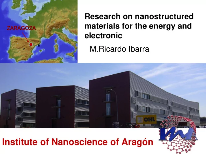
M.Ricardo Ibarra
M B
Institute of Nanoscience of Aragn OUTLINE -Presentation of the - - PowerPoint PPT Presentation
Research on nanostructured materials for the energy and electronic B M.Ricardo Ibarra M Institute of Nanoscience of Aragn OUTLINE -Presentation of the Institute of Nanoscience of Aragn -Nanomaterials research in Aragn INSTITUTE OF
M B
NANOBI OMEDI CI NE: NANOBI OMEDI CI NE:
Therapy: :
Drug Delivery Delivery
Hypertherm y
Diagnó óstic stic: :
Contrast agent agent ( ( biom olecular biom olecular and and celular celular targeting targeting) )
Biosensors: : Quantitative Quantitative lateral lateral flow flow . . NANOSTRUCTURED MATERI ALS: NANOSTRUCTURED MATERI ALS:
Mem branes and and nanoporous nanoporous film s film s
Carbon nanotubes nanotubes
Organic functionals functionals m aterials m aterials ( ( dendrim ers dendrim ers, , m esosocopic m esosocopic liquid liquid crystals crystals
Core-
shell m agnetic m agnetic nanoparticles nanoparticles PHYSI CS AT THE NANOSCALE: PHYSI CS AT THE NANOSCALE:
Thin film s film s: : m agnetic m agnetic heteroestructures heteroestructures, , superlattices superlattices… …
Micro-
Nanocircuits: : Spintronics Spintronics, quantum , quantum effects effects, , nanow ires nanow ires, , nanoconstrictions nanoconstrictions, , MEMS&NEMS MEMS&NEMS... ...
INSTITUTE OF NANOSCIENCE OF ARAGON INSTITUTE OF NANOSCIENCE OF ARAGON RESEARCH LINES RESEARCH LINES
ABLATION
Fe3 O4 / MgO epitaxial thin film
PRESENT (20 m2, CLASS 10.000) NEW (125 m2, CLASS 10.000 & CLASS 100)
saw
MASK ALIGNER PHOTORESIST STATION MICROCONTACTS ELECTRON BEAM EVAPORATOR
DRY ETCHING RIE/IBE
LHe cryostat Ion gun STM head LEED - Auger Evaporators Quadrupole mass spectrometer UHV sample preparation chamber
TiO TiO
2 2
LEED pattern from a Cu (1 1 13) surface (regular array of steps)
HRTEM: FEI TECNAI G2 F30
Fe SiO
2
Fe Fe SiO
2
UHRTEM: Cs correctors (Future project)
Imaging Ectching Deposition Analysis Nanopatterning e-beam lithography
Orbital shaker Celules and bacterials separation Virus and DNA separation Peptide chromatography U-V spectrometer Cell culture&nanoparticles
10 20 30 40 50 60 70
5 10 15 20 25
1.00 % wt 0.67 % wt 0.50 % wt 0.25 % wt
T - T (t=0) ºC
Tiempo (min)
Magnetic Hyperthermy Anatomopatology
Veterinary Hospital Suregery room Endoscopic surgery
Nanoparticles Optical microscopy Laminar flow cabine
X X-
RAY DIFFRACTION HIGH RESOLUTION D8 Brucker Brucker
10 10
110
210
310 4 10 5 10 6 10
741 41.5 42 42.5 43 43.5 44 44.5 45
Counts 2θ (deg) 002 MgO 004 Fe 3O4 Laue oscillations
Laue oscillations high degree
10
110 2 10
310
410
50.5 1 1.5 2 2.5 3 3.5 4
Counts 2θ (deg) Thickness = 40.0 nm
X-ray reflectivity
740 735 730 725 720 715 710 705 700 0,0 0,2 0,4 0,6 0,8 1,0 1,2 1,4 1,6 satélite Fe
2+
729.3 eV satélite Fe
3+
733.7 eV satélite Fe
2+
715.7 eV
Fe 2p1/2 Normalized Intensity BE (eV) magnetita wüstita (mezcla) hematita
Fe 707eV
Fe 2p 3/2
711.2 eV satélite Fe
3+
719.7 eV 710.2 eV
Iron ionic states in different oxides
Temperature range 100 K -800 K High sensitivity (~10-6 emu). Magnetic field up to 2 Tesla
Hystheresis loops of a epitaxial Fe thin film with the field applied along [100] y [110] directions
O4 , Sr2 CrReO6
The tool: UHV combined PLD-sputtering system
New chambers to be installed before June 2009: dedicated PLD + dedicated sputtering
High-quality Thin Films / Heterostructures succesfully grown to date:
O4
O4 /MgO/Fe
CrReO6
O4
100 µm 100 µm
500 nm 500 nm
SiO2 Fe microprobes
100 µm 100 µm
500 nm 500 nm
100 µm 100 µm
500 nm 500 nm
SiO2 Fe microprobes
2 4 6 8 4 6 8 10 end depos. Pt-C start depos. Pt-C end etching
R (kΩ) t (min)
start etching
2 4 1 2 3 H ⏐⏐ I 24K 30K 35K
MR(%) H(kOe) P AP
2 4 1 2 3 H ⏐⏐ I 24K 30K 35K
MR(%) H(kOe) P AP
Two Polymer Families to withstand hight temperatures have been proposed: Polyetherimides (PEI), polysulfones (PSU)
degradation
25
BENEFITS OF T INCREASE PROBLEMS/SPECIFIC CHALLENGES
26
I ONI C LI QUI DS Advantages
conductivity
Disadvantages
into a matrix to be used as an electrolyte
POLYMERS Advantages
fragile)
Disadvantages
ZEOLI TES Advantages
stability
humidification is not necessary for proton conduction)
structures, tailor made porosity and modulable adsorption properties (fuel-cross over)
Disadvantages
conductivity
(fragility)
27
ZEOLITES & MICROPOROUS RELATED MATERIALS IMIDAZOLIUM/ AMMONIUM BASED IONIC LIQUIDS
(PEI, PSU, s-PEEK, doped PBI)
IONIC LIQUID ZEOLITE MEMBRANE POLIMERIC MATRIX
(top view) (cross section)
(ordered or randomly porous membranes)
Eutectics are a paradigm for pattern structures of size scales down to submicron and nanometer with clean interfaces.
2009
YAG YAG YAG Growth direction Al2 O3 Al2 O3 YSZ YSZ YSZ YSZ PB Oliete et al. Adv. Mat (2007)
Microstructure of LFZ fabricated Al2O3-YAG-YSZ ternary eutectic
Á Ánodo nodo :400 :400-
500 µ µm m Electrolito 10 Electrolito 10 -
20 µ µm m C Cá átodo: 8 todo: 8 µ µm m (LSM + (LSM + YSZ) YSZ) Fuel: 4% H2 2009
50 100 150 200 250 300 350 400 450 500 550 600 650 100 200 300 400 500 600 700 800 900 1000 50 100 150 200 250 300 350 400
Power(mW/cm
2)
Voltage(mV) Intensity(mA/cm
2)
650ºC 700ºC 750ºC 800ºC 850ºC 900ºC
Directionally Solidified Eutectics
self-organized lamellar microstructure & Strong interphase bonding Channeled M-YSZ cermet Easy gas flow High electronic conductivity Same CTE as YSZ Microstructural stability
1 R.I. Merino et al., J. Eur.. Ceram. Soc. 2005, 25, 1455-1462. 2 M.A. Laguna-Bercero et al., J. Eur.. Ceram.
3 G. García et al., Chem. Vap. Deposition 2004,
10 249-252
YSZ electrolyte deposited by CVD on a Ni-YSZ channeled cermet Fracture of a Ni-YSZ channeled cermet
Department of Nanotechnology
Development of novel electroactive polymer/nanotube composite materials
For use as
Active organic layer PEDOT/PSS+ CNT vidrio ITO Al Al Au Au
+ TOWARDS Flexible and efficient Photovoltaic Cells
Patent: PCT/ES2009/070021
NANOTUBES AND RENEWABLE ENERGY APPLICATIONS
Department of Nanotechnology
+
Patent: PCT/ES2009/070021
Development of novel conducting polymer/nanotube composite materials
For use as
In Supercapacitors and Batteries TOWARDS Flexible and efficient electrochemical devices NANOTUBES AND RENEWABLE ENERGY APPLICATIONS
Department of Nanotechnology
Production of TiO2 nanotubes
For use : Hydrogen production Organic contaminants degradation
NANOTUBES AND RENEWABLE ENERGY APPLICATIONS Photacatalysis mechanism TiO2 Nanotubes TiO2 Nanotubes