SLIDE 1
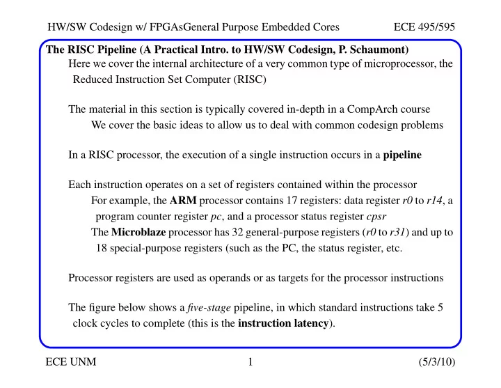
HW/SW Codesign w/ FPGAsGeneral Purpose Embedded Cores ECE 495/595 ECE UNM 1 (5/3/10) The RISC Pipeline (A Practical Intro. to HW/SW Codesign, P. Schaumont) Here we cover the internal architecture of a very common type of microprocessor, the Reduced Instruction Set Computer (RISC) The material in this section is typically covered in-depth in a CompArch course We cover the basic ideas to allow us to deal with common codesign problems In a RISC processor, the execution of a single instruction occurs in a pipeline Each instruction operates on a set of registers contained within the processor For example, the ARM processor contains 17 registers: data register r0 to r14, a program counter register pc, and a processor status register cpsr The Microblaze processor has 32 general-purpose registers (r0 to r31) and up to 18 special-purpose registers (such as the PC, the status register, etc. Processor registers are used as operands or as targets for the processor instructions The figure below shows a five-stage pipeline, in which standard instructions take 5 clock cycles to complete (this is the instruction latency).
SLIDE 2
HW/SW Codesign w/ FPGAsGeneral Purpose Embedded Cores ECE 495/595 ECE UNM 2 (5/3/10) RISC Pipeline: Operation and Hazards Each dashed line represents a pipeline register Instruction Fetch: an instruction is retrieved from memory or the instruction cache Instruction Decode: an instruction is decoded and the register operands for this instruction are fetched. Branch instructions will modify the PC during this phase
SLIDE 3 HW/SW Codesign w/ FPGAsGeneral Purpose Embedded Cores ECE 495/595 ECE UNM 3 (5/3/10) RISC Pipeline: Operation and Hazards Execute: the operands are input to the datapath operators and executed Buffer: the data memory is accessed using an address generated in the execute phase Write-back: registers are updated to reflect the final result of the instruction execu- tion In an ideal situation, the architecture above can complete 1 instruction per clock cycle (this is instruction throughput) Even though instruction latency is 5 clock cycles, the pipeline enables over- lapped execution of these instructions to increase throughput The clock cycle time is limited by the slowest component in the pipeline, plus the
- verhead of the pipeline registers (clock skew and setup)
If a pipeline stage is too slow, additional pipeline stages can be added spreading the computation over multiple clock cycles Doing so also extends the instruction latency
SLIDE 4 HW/SW Codesign w/ FPGAsGeneral Purpose Embedded Cores ECE 495/595 ECE UNM 4 (5/3/10) RISC Pipeline: Operation and Hazards The ideal situation of one instruction per clock cycle is the best case scenario A pipeline stall occurs when the progress of instructions through the pipeline is tem- porarily halted The cause of such a stall is a pipeline hazard Pipeline interlock hardware can detect pipeline hazards and resolve them automati- cally in many cases, but stalls still occur There are several types of pipeline hazards We discuss these in the context of examples from a ARMv6 processor The following generalizations can be made:
- Control hazards are caused by branches
- Data hazards are caused by unfulfilled data dependencies
- Structural hazards are caused by resource conflicts and cache misses
SLIDE 5
HW/SW Codesign w/ FPGAsGeneral Purpose Embedded Cores ECE 495/595 ECE UNM 5 (5/3/10) Control Hazards Branches are the most common form of pipeline stalls As shown in the pipeline architecture, a branch is only executed in stage 2 of the pipeline When this occurs, another instruction has already entered the pipeline This instruction follows the branch instruction sequentially, so if the branch is taken, its execution needs to be cancelled The next slide illustrates a control hazard The pipeline is shown drawn on its side, running from left to right and time runs down across the rows A control hazard occurs because of the branch instruction ble TGT In cycle 2, the new program counter value evaluates to the target address of the branch, TGT
SLIDE 6
HW/SW Codesign w/ FPGAsGeneral Purpose Embedded Cores ECE 495/595 ECE UNM 6 (5/3/10) Control Hazards
SLIDE 7
HW/SW Codesign w/ FPGAsGeneral Purpose Embedded Cores ECE 495/595 ECE UNM 7 (5/3/10) Control Hazards Note that ble is a conditional branch that uses the result of the instruction just before that (cmp r0, #5) And the interlock hardware in the pipeline makes the branch condition available in cycle 2 The instruction following the branch is cancelled in the decode stage, and the unused slot progress through the remaining pipeline stages Starting in cycle 3, instructions from the target address TGT enter the pipeline Some processors (including the Microblaze) have a branch-delay instruction A branch-delay instruction that allows the instruction following the branch to com- plete even when the branch is taken The instruction inserted into the branch-delay slot must be an instruction that would execute independent of the branch The compiler can automatically determine candidate instructions for the slot -- if none exist, a NO-OP instruction is inserted
SLIDE 8
HW/SW Codesign w/ FPGAsGeneral Purpose Embedded Cores ECE 495/595 ECE UNM 8 (5/3/10) Control Hazards This fills in the stall slots with execution of an instruction at X+4 int accumulate() { int i, j; for (i=0; i<100; i++) j += i; return j; } Compiling generates the following assembly code for Microblaze: addk r4,r0,r0 ;clear r4 (holds i) addk r3,r3,r4 ;j = j + i $L9: addik r4,r4,1 ;i = i + 1 addik r18,r0,99 ;r18 <- 99 cmp r18,r4,r18 ;compare i and 99 bgeid r18,$L9 ;delayed branch if not equal addk r3,r3,r4 ;j = j + i (branch delay slot)
SLIDE 9
HW/SW Codesign w/ FPGAsGeneral Purpose Embedded Cores ECE 495/595 ECE UNM 9 (5/3/10) Data Hazards Registers are updated only during the write-back phase However, it is possible that a register value is required before that value has reached the write-back phase Consider the instructions: MOV r0, #5 ADD r1, r0, r1 By the time the MOV instruction reaches the write-back stage, the ADD instruction will be in the buffer stage, and the addition would have already completed This situation will be detected by the pipeline interlock, which will stall part of the pipeline When the data becomes available, it will be directly forwarded to the execution stage where it is needed
SLIDE 10
HW/SW Codesign w/ FPGAsGeneral Purpose Embedded Cores ECE 495/595 ECE UNM 10 (5/3/10) Data Hazards In some cases, forwarding is NOT possible b/c the data is simply not yet available This happens when a read-from-memory instruction is followed by an instruc- tion that uses the data coming from memory
SLIDE 11
HW/SW Codesign w/ FPGAsGeneral Purpose Embedded Cores ECE 495/595 ECE UNM 11 (5/3/10) Data Hazards The second instruction fetches data from memory and stores it in register r1 The following add instruction uses the data from that register as an operand In cycle 4, the add instruction reaches the execute stage However, at that moment, the ldr instruction is still accessing the data memory The new value of r1 is only available at the start of cycle 5 Therefore, the interlock hardware will stall all stages preceding the buffer stage in cycle 4 Data hazards can lengthen the execution time of an instruction For classic RISC processors, data hazards can be predicted statically, by examining the assembly program When the execution time of a program needs to be estimated exactly, a programmer will need to be able to identify all data hazards and their effects
SLIDE 12
HW/SW Codesign w/ FPGAsGeneral Purpose Embedded Cores ECE 495/595 ECE UNM 12 (5/3/10) Structural Hazards Structural Hazards are caused by instructions that require more resources than the processor has available These cause stalls to be introduced into the pipeline, similar to data and control hazards
SLIDE 13 HW/SW Codesign w/ FPGAsGeneral Purpose Embedded Cores ECE 495/595 ECE UNM 13 (5/3/10) Structural Hazards Here, the ldmia instruction is a load-multiple instruction that will read consecu- tive memory locations and store the resulting values in memory In the example shown, the value stored in address r0 will be copied to r1, while the value stored in address r0+4 will be copied to r2 When the ldmia instruction reaches the execute stage, the execute stage will be busy for two clock cycles in order to evaluate the memory addresses r0 and r0+4 Therefore, all pipeline stages before the execute stage are halted for a single clock cycle A structural hazard is caused by the processor architecture, but it may have a wider range of causes
- The width of memory ports
- The number of execution units in the data-path
- Restrictions on the communication busses
SLIDE 14 HW/SW Codesign w/ FPGAsGeneral Purpose Embedded Cores ECE 495/595 ECE UNM 14 (5/3/10) Structural Hazards A programmer can only predict structural hazards through a solid understanding of the processor architecture Furthermore, memory latency effects can also cause the execution time of the buffer stage to vary A cache miss for example can extend the latency of a load-memory instruction to hundreds of cycles Program Organization Here, we will look at the relationship between a C program and its implementation
This includes:
- A discussion of the main parts of a C program and their mapping to instructions and
into sections of memory
- The organization of a C program into binary format
- And the link between a C program and the RISC architecture
SLIDE 15
HW/SW Codesign w/ FPGAsGeneral Purpose Embedded Cores ECE 495/595 ECE UNM 15 (5/3/10) Program Organization While the examples will be made for ARM and MicroBlaze RISC processors, the ideas explained here are generic and applicable to many other RISC processors A good hardware/software codesigner tries to be as architecture-independent as possible, to enable easy movement between architectures In fact, it is possible to do a decent performance analysis of a C program at the cycle- accurate level, without detailed knowledge of the instruction-set of a processor Data Types C program data types are a good starting point to discuss the mapping of C programs to RISC processors The following table shows how C maps to the native data types supported by ARM and Microblaze processors All C data types, apart from char, are treated as signed (two’s complement) numbers
SLIDE 16
HW/SW Codesign w/ FPGAsGeneral Purpose Embedded Cores ECE 495/595 ECE UNM 16 (5/3/10) Program Organization (Data Type) The difference between operations on two’s complement (signed) numbers and oper- ations and unsigned numbers is minor Signed numbers may require sign extension In addition, the comparison of signed numbers is different from the comparison of unsigned numbers When comparing unsigned bytes, 0xff is bigger then 0x01, but is smaller for signed numbers
SLIDE 17
HW/SW Codesign w/ FPGAsGeneral Purpose Embedded Cores ECE 495/595 ECE UNM 17 (5/3/10) Program Organization (Data Type) The mapping of C data types to physical memory locations is affected by several fac- tors First, data types need to follow the rules of data type alignment, which define what are the allowed starting addresses for data types in memory A RISC processor will access the data memory at pre-defined physical boundaries, typically one word (32 bits) at a time Thus, a single memory transfer may be able to access any of the four bytes in a word But a group of four bytes across a word boundary cannot be accessed in a sin- gle memory transfer For this reason, data types may need alignment in the physical memory organization, and this restricts the location of these data types in logical address space
SLIDE 18
HW/SW Codesign w/ FPGAsGeneral Purpose Embedded Cores ECE 495/595 ECE UNM 18 (5/3/10) Program Organization (Data Type) A second factor that affects the mapping of data types is the storage order (see Figure 6.7b) A little-endian storage order will map the least significant bytes of a word into lower memory locations (big-endian storage order is the opposite)
SLIDE 19
HW/SW Codesign w/ FPGAsGeneral Purpose Embedded Cores ECE 495/595 ECE UNM 19 (5/3/10) Program Organization (Data Type) In C, you do not need to worry about the endianess In hardware/software codesign, the physical representation of data types is important in the transition of software to hardware and back Hence, the endianess of a processor (and in some cases even the bit-ordering) is important It is easy to check the endianess of a given processor using a small C program: int main() { char j[4]; volatile int *pj; pj = (int *) j; j[0] = 0x12; j[1] = 0x34; j[2] = 0x56; j[3] = 0x78; printf("‰x\n", *pj); }
SLIDE 20 HW/SW Codesign w/ FPGAsGeneral Purpose Embedded Cores ECE 495/595 ECE UNM 20 (5/3/10) Program Organization (Data Type) For this program
- A little-endian processor will print 78563412
- A big-endian processor will print 12345678
Microblaze processor is big-endian, while an ARM processor is (normally) little- endian