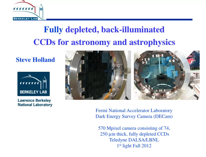
fully depleted back illuminated
play

Fully depleted, back-illuminated CCDs for astronomy and astrophysics - PowerPoint PPT Presentation

Fully depleted, back-illuminated CCDs for astronomy and astrophysics Steve Holland Fermi National Accelerator Laboratory Dark Energy Survey Camera (DECam) 570 Mpixel camera consisting of 74, 250 m thick, fully depleted CCDs Teledyne


  1. Fully depleted, back-illuminated CCDs for astronomy and astrophysics Steve Holland Fermi National Accelerator Laboratory Dark Energy Survey Camera (DECam) 570 Mpixel camera consisting of 74, 250 µm thick, fully depleted CCDs Teledyne DALSA/LBNL 1 st light Fall 2012

  2. Outline • Fundamentals of CCDs and CMOS image sensors • Scientific CCDs for astronomy • Fully depleted CCDs fabricated on high-resistivity silicon – device physics/applications/technology

  3. Scientific CCDs vs cell phone imager Unofficial comparison, scientific CCD versus CMOS image sensor for cell phones (e.g. iPhone 4, TSMC/OmniVision 1 ) Parameter CMOS cell phone Scientific CCD 8 – 16 Megapixels # pixels 5 - 8 Megapixels 1.4 – 1.7 µm 10 – 15 µm Pixel size 15 mm 2 (5M) 3775 mm 2 (16M) Imaging area Technology 130 nm CMOS 2.5 µm CCD Illumination Back illumination Back illumination 10 – 250 µm Optical thickness ~ 3 µm ~ 90 – 95% ~ 55% (color filter) Peak QE -100°C – -140°C Operating temp Up to 50°C 20 – 30 e-/pixel/sec Dark current Few e-/pixel/hr Read noise ~ 2 e- ~ 2-5 e- Full well ~ 4500 e- ~ 200,000 e- (15 µm) 1 Rhodes, 2009 IISW Symp. On Backside Illumination of Solid-State Image Sensors, imagesensors.org and http://image-sensors-world.blogspot.com/2010/06/iphone-4-bsi-sensor-is-omnivisions.html

  4. Scientific CCDs vs cell phone imager Unofficial comparison, scientific CCD versus CMOS image sensor for cell phones (e.g. iPhone 4, TSMC/OmniVision 1 ) Parameter CMOS cell phone Scientific CCD 8 – 16 Megapixels # pixels 5 - 8 Megapixels 1.4 – 1.7 µm 10 – 15 µm Pixel size 15 mm 2 (5M) 3775 mm 2 (16M) Imaging area Technology 130 nm CMOS 2.5 µm CCD Illumination Back illumination Back illumination 10 – 250 µm Optical thickness ~ 3 µm ~ 90 – 95% ~ 55% (color filter) Peak QE -100°C – -140°C Operating temp Up to 50°C 20 – 30 e-/pixel/sec Dark current Few e-/pixel/hr Read noise ~ 2 e- ~ 2-5 e- Full well ~ 4500 e- ~ 200,000 e- (15 µm) Cost << ~

  5. CCD 101 – Invention • Invented by W. Boyle and G. Smith (Bell Laboratories) on September 8 th , 1969 – Awarded Nobel Prize in Physics 2009 • Tasked by Jack Morton to find a semiconductor analogy to the magnetic “bubble memory” • The basic concepts were conceived in a discussion session between Boyle and Smith “lasting not more than an hour” 1-3 [1] G.E. Smith, “The invention and early history of the CCD,” J. Appl. Phys., 109, 102421, 2011. [2] W.S. Boyle and G.E. Smith, “The inception of charge -coupled devices,” IEEE Trans. Elec. Dev., 23, 661, 1976. [3] G.E. Smith, “The invention of the CCD”, Nucl. Instrum. Meth. A, 471, 1, 2001.

  6. CCD 101 – Boyle/Smith notebook entry • Collection and storage of charge in MOS capacitor depletion regions — Dashed line denotes edge of depletion region — + denotes storage of charge (holes in this case) • Charge transferred via clocking of closely spaced electrodes 3-phase CCD diagram (lab notebook drawing Sept. 1969)

  7. 2D simulation of charge shift in CCD

  8. CCD 101 – Triple poly process Scientific CCDs typically use the same 3-phase clocking as in the original Boyle and Smith concept with overlapping polysilicon gate electrodes (triple poly) Poly 2 Poly 3 Poly 1

  9. CCD 101 UC-Berkeley connections to CCD development IEEE Trans. Elec. Dev., 21, 712, 1974 Carlo Sequin, UC-Berkeley Professor of Computer Science since 1977

  10. CCD 101 For maximum quantum efficiency scientific CCDs are back illuminated

  11. Front vs Back illumination – CCDs Front illumination: Quantum efficiency loss from • Absorption in polysilicon gates • Reflections from complicated thin film stack Back illumination (thinned CCDs): • Remove p+ substrate • Limited depletion depth for typical resistivity silicon implies significant thinning (10 – 20 µm for scientific CCDs, ~ 3 µm for CMOS image sensors)

  12. Front vs Back illumination – CCDs Sloan Digital Sky Survey CCD quantum efficiency versus wavelength comparing 1) Back illumination 2) Front illumination

  13. CCD vs CMOS image sensor • CCDs: Shifting of charge vertically and horizontally to a source follower amplifier that converts charge to voltage • CMOS image sensors have an SF amplifier in each pixel eliminating the need for high charge-transfer efficiency A. Theuwissen, IEEE Solid-State Circuits Magazine, 22, Spring 2010

  14. CCD 101 – CMOS image sensor • CMOS image sensors incorporate pinned photodiodes 1 to suppress surface dark current and floating diffusion amplifiers • kTC noise suppression – Borrowed from CCDs Analogous to buried channel CCD potential profile A. Theuwissen, IEEE Solid-State Takayanagi and Nakamura, to Circuits Magazine, 22, Spring 2010 appear in IEEE Proceedings 1 N. Teranishi et al, IEEE Trans. Elec. Dev., 31 , 1829, 1984

  15. Front vs back illumination – CMOS • CMOS image sensors with small pixels need back illumination simply to get the light into the pixel IBM front illuminated CMOS image sensor Sony back illuminated CMOS image sensor 2.2 µm pixel 1.65 µm pixel 2006 IDEM (Gambino et al) 2010 ISSCC (Wakabayashi et al)

  16. Outline • Fundamentals of CCDs and CMOS image sensors • Scientific CCDs for astronomy • Fully depleted CCDs fabricated on high-resistivity silicon – device physics/applications/technology

  17. Scientific CCDs for Astronomy • Scientific charge-coupled devices are the detector of choice for astronomy applications in the UV, visible and near-infrared wavelengths λ ~ 350 nm to about 1.1 µm (atmospheric cutoff to Si bandgap) — Back illuminated for high quantum efficiency > 90% peak — Slow readout for low noise < 5 e- typically at 100 kpixels/sec readout

  18. Scientific CCDs for Astronomy • Scientific charge- coupled devices (cont’) — Cryogenically cooled for low dark current Few electrons/pixel-hour at -100 to -140ºC — Large format with large pixels 10 – 15µm pixels, 4k x 4k and larger — Very $$$ Examples of astronomy cameras follow

  19. CCD cameras for astronomy 120 Mpixels SDSS Photometric Camera – 30 2k x 2k, (24 µm) 2 -pixel CCDs Sloan Digital Sky Survey Telescope / 2000 – 2008 Thinned (~ 10 – 20 µm thick), partially depleted CCDs from SITe

  20. CCD cameras for astronomy ~ 6 cm ~ 3 cm 256 Mpixels 340 Mpixels MegaCam – 36 2k x 4k, (15 µm) 2 -pixel CCDs OmegaCAM – 32 2k x 4k, (15 µm) 2 -pixel CCDs Canada-France-Hawaii Telescope / 2003 ESO VLT Survey Telescope (VST) 1 st light June 2011 Thinned (~ 10 – 20 µm thick), partially depleted CCDs from e2V

  21. CCD cameras for astronomy (cont’) 1.4 Gpixels 64 Mpixels SuprimeCam – 8 2k x 4k, (15 µm) 2 -pixel CCDs PS1 camera – 60 4.8k x 4.8k, (10 µm) 2 -pixel CCDs Subaru 8-m Telescope (1998) Pan-STARRS telescope (2010) ~ 40 µm thick, partially depleted and ~ 75 µm thick, fully depleted CCDs (deep depletion CCDs) MIT Lincoln Laboratory

  22. CCD cameras for astronomy (cont’) 870 Mpixels 84 Mpixels SuprimeCam – 10 2k x 4k, (15 µm) 2 -pixel CCDs HyperSuprimeCam – 116 2k x 4k, (15 µm) 2 -pixel CCDs Subaru 8-m Telescope (2008) Subaru 8-m Telescope 1 st light achieved 28Aug2012 ~ 200 µm thick, fully depleted CCDs Hamamatsu Corporation

  23. Coming soon – Fermi National Accelerator Laboratory Dark Energy Survey Camera 520 Mpixels Dark Energy Survey Camera (DECam) – 62 2k x 4k, (15 µm) 2 -pixel CCDs NOAO Cerro Tololo Blanco 4-m Telescope (Fall 2012) 250 µm thick, fully depleted CCDs (DALSA/LBNL)

  24. Coming soon – Fermi National Accelerator Laboratory Dark Energy Survey Camera Credit: CTIO/AURA/NSF Artist’s rendering – Cerro Tololo Inter-American Observatory V. M. Blanco 4-m telescope (Chile)

  25. Coming soon – Fermi National Accelerator Laboratory Dark Energy Survey Camera

  26. Coming soon – Fermi National Accelerator Laboratory Dark Energy Survey Camera DECam's imager is visible for the last time (blue, left of center) before it is inserted into the instrument, meeting the optical corrector for the first time. Image credit: T. Abbott CTIO/NOAO/AURA.

  27. DES Collaboration … is an international project to “nail Fermilab, UIUC/NCSA, University of Chicago, down” the dark energy equation of state. LBNL, NOAO, University of Michigan, University of Pennsylvania, Argonne National Laboratory, Ohio State University, Santa-Cruz/SLAC Consortium, Texas A&M UK Consortium: UCL, Cambridge, Edinburgh, Portsmouth, Sussex Ludwig-Maximilians Universität LMU Spain Consortium: CIEMAT, IEEC, IFAE Brazil Consortium: Observatorio Nacional, CBPF,Universidade Federal do Rio de 119+ scientists Janeiro, Universidade Federal do Rio 12+ institutions CTIO Grande do Sul

  28. Outline • Fundamentals of CCDs and CMOS image sensors • Scientific CCDs for astronomy • Fully depleted CCDs fabricated on high-resistivity silicon – device physics /applications/technology

  29. Fully depleted, back-illuminated CCD 1) Concept: Fabricate a conventional CCD on a thick, high-resistivity Si substrate (> 4 k Ω -cm) 200-250 µm typical 2) Use a substrate bias voltage to fully deplete the substrate of mobile charge carriers Merging of p-i-n and CCD technology High- ρ Si allows for low depletion voltages Float-zone refined silicon

Download Presentation
Download Policy: The content available on the website is offered to you 'AS IS' for your personal information and use only. It cannot be commercialized, licensed, or distributed on other websites without prior consent from the author. To download a presentation, simply click this link. If you encounter any difficulties during the download process, it's possible that the publisher has removed the file from their server.

Recommend


More recommend