
SLIDE 1
- .kurnosikov@tue.nl
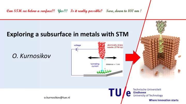
Can STM see below a surface?! Yes!!! Is it really possible? Sure, down to 100 nm !
Exploring a subsurface in metals with STM
- O. Kurnosikov
Exploring a subsurface in metals with STM O. Kurnosikov - - PowerPoint PPT Presentation
Can STM see below a surface?! Yes!!! Is it really possible? Sure, down to 100 nm ! Exploring a subsurface in metals with STM O. Kurnosikov o.kurnosikov@tue.nl Introduction: Scanning Tunneling Microscopy/Spectroscopy In selected points For
7.8Å
Cu(111)
reflects the Density of States
Resolution Lateral : atomic, ~0.1nm Vertical : subatomic, ~0.001nm
Two ways of get the subsurface sensibility:
density
Co nanoclusters embedded below Cu(001) surface, 75 x 75 nm 2.
20 pm
Ar bubble below Cu(001) surface, 30 x 15 nm 2.
Deformation
Mismatch of crystalline lattices of substrate and impurity atoms or embedded nanocluster . Relaxation of crystalline lattice and interaction of embedded atoms
[110] [110]
60×60 nm2
500mV 600mV 500mV 400mV
60×60 nm2
Ar nanocavities in Cu(001), the same area, different bias Ar nanocavities in Cu(110), the same area, different bias What we have and what we see
1 2 3 4 1 2 3 4
DE110 DEss
if ΔΕ=0,25 mV then d = 12 nm
Ar-, Ne- or He- filled nanocavities have much stronger scattering effect and therefore they can be detected much dipper than single impurities
visualized in STM measurements as spots of different contrast above their locations. The contrast
nanocavities induce different
this the shape and size of the nanocavity can be determined.
Studied system
Shape: different spots – different facets
20 x 20 nm2
39.0 nm 52.9 nm 62.8 nm 80.0 nm 4.5 nm 12.5 nm 22.4 nm 32.5 nm
Depth
40 x 40 nm
10 nm of Cu
dI/dV @ 900mV
Co nanoclusters in Cu(001)
dI/dV @ 400mV
6 nm of Cu
30 x 30 nm
Fe nanoclusters in Cu(001)
Nanocavities vs Nanoclusters Applications
For ITER Degradation of W or Mo walls by implantation and growth of H2 and He-filled nanocavities: the growth
For micro- nanolithography Ar, Ne, He implantation defects in conducting layers (Al, Cu, Au, Ag, …) during plasma processing
For clean material technology Study near-surface defects and interfaces directly or by decoration them with He or H nanocavities For solar cells and nanophotonics Ge nanoclusters and nanovoids in fused silica Metallic clusters provide less effective scattering. Nevertheless we can see Co and Fe nanoclusters up to 25 nm deep.
10/31/2019 6
20 x 20 nm
/ Acta Materialia 90 (2015) 370–379
Pure tungsten
ArXiv 1712.05308.pdf
Tungsten with impurities Our experiments
Estimated size ~15 nm
6
0,0 0,2 0,4 0,6 0,8 1,0 1,2 0,6 0,7 0,8 0,9 1,0 1,1 1,2 1,3 1,4
(dI/dV)/dIo/dV) Bias voltage, V G 0.22mV
~10 nm