
SLIDE 1
Sam Jewell, G4DDK EME 2016 Venice, August 2016
1
EME 2016 Venice, August 2016 1 Failure levels in LNAs Update on - - PowerPoint PPT Presentation
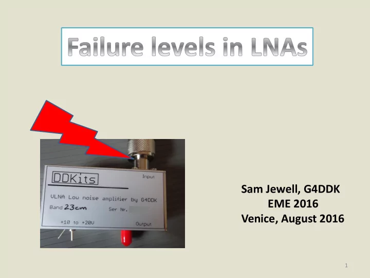
Sam Jewell, G4DDK EME 2016 Venice, August 2016 1 Failure levels in LNAs Update on the VLNA Investigation of the failures seen in the VLNA Nature of the failures Method of the investigation Results Conclusions
1
2
3
0,05 0,1 0,15 0,2 0,25 0,3 0,35 0,4 0,45 500 1000 1500 2000 2500 3000 3500 4000 Noise figure (dB) Frequency (MHz)
Typical VLNA noise figure
4
5 10 15 20 25 30 35 40 432 1296 2320 3400 Gain (dB) Frequency (MHz)
Typical gain
5
6
~1.6V 2.94V 66mA 15mA
7 2.7pF 8.2pF 13nH 2.7nH LNA input Active device
Input noise matching circuit for the VLNA23
8
9
10
– ATF53189 PHEMT has been shown to exhibit the same effect at 2m
11
12
13
14
15
16
0,1 1 10 100 5 10 15 20 Noise figure and gain (dB) Input level (dBm)
Early results - Power on Table 1,2,3,&4
Noise figure increase Noise figure fail
17
0,1 1 10 100 5 10 15 20 Noise figure and gain (dB) Input level (dBm)
Early results - power off Table 4*,5 and 6
*Two table 4! Noise figure increase Noise figure fail
18
19
0,1 1 10 100 5 10 15 20 Noise figure & gain (dB) Input power (dBm)
Latest results - Power ON
20
0,1 1 10 100 5 10 15 20 Noise figure & gain (dB) Input power (dBm)
Latest results - Power OFF
21
22
23
24
25
120R = 10V @85mA Preamp and isolation relay Powered in parallel Option to use 20-24V
26
More details will appear on my web page G4DDK.COM Blog: G4DDK.BLOGSPOT.COM Twitter: DXING
27