
ASICs for Belle II DEPFET Pixel Detector
....
- I. INTRODUCTION
D
EPFET pixel modules will be readout in ’rolling shutter mode’, which means that the rows (precisely 4-row matrix segments) are selected consecutively and all columns are read
- ut in each readout cycle. Three different ASIC types will be
used for the readout. The SWITCHER steering chips are selecting and clearing the DEPFET 4-row segments by generating their external gate- and clear voltages. The readout of the columns is done by Drain Current Digitizer (DCD) chips, placed at the bottom of each half-module matrix. These chips receive, process and digitize the current signals generated by the DEPFETs of the selected matrix segment. The eight-bit ADC codes are then sent to the Data Handling Processors (DHPs) that perform data processing, compression, buffering and fast serialization. All the chips will be mounted directly on the detector module using bump-bonding and flip-chip techniques leading to fully- silicon modules.
- II. SWITCHER
The SWITCHER steering chips will be mounted on the about 2 mm-wide, inactive 300 µm-thick edge rim of the DEPFET
- module. These chips provide fast (10 ns into 50 pF) voltage
pulses of up to 20 V-amplitude to activate gate rows and to clear the internal DEPFET gates. SWITCHER is implemented in standard AMS 0.18 µm or 0.35 µm HV technology. One SWITCHER will be able to ’address’ 32 different DEPFET matrix segments (row groups), for this purpose it will have 32 ’channels’ with a clear- and a gate-driver each. One row group is selected by pulling the external gates at a negative voltage which switches the pixels on. Clearing is achieved by puling the clear diffusion of the selected DEPFETs at a positive voltage. The SWITCHER channels and their drivers are activated consecutively. Readout of one DEPFET half- module with 192 row groups (768 pixel rows) would require six SWITCHERs. All required SWITCHER control signals and power run on the only 2 mm-wide module rim. The number of I/O signals has therefore been minimized and an unusual bump pad geometry has been chosen to simplify routing on the module - the bump array is placed in the middle of the chip. In order to simplify system design, the SWITCHERs have a floating digital ground and use fast, low power level shifters. A JTAG interface allows for interconnectivity tests on the module. The design of the SWITCHER versions optimized for Belle-II requirements (SWITCHERB18 in 0.18 µm and SWITCHERB in 0.35 µm) has been finished. Both chips have been successfully tested. Radiation hardness of at least 37 MRad has been demonstrated.
- III. DCD
The currents generated by a selected DEPFET row-group are routed out via column lines and readout by the DCD chips placed at the bottom of each half-module matrix. Each DCD has 256 analog inputs. Since one row-group consists of 1024 DEPFET pixels (four rows with 256 pixels each), four DCDs will be needed to readout all the columns in parallel. There will be therefore eight DCD chips on a module. DCD is implemented in UMC 0.18 µm CMOS technology using special radiation hard design techniques. The chip occupies 3.2 mm × 5 mm area. Chip size and input pitch have been adapted to the specific Belle-II requirements. DCD-B uses bump bonding on the UMC technology provided by EuroPractice. DCD has 256 analog channels each housing an input stage and two ADCs. The analog input stage performs various
- tasks. It keeps the column line potential constant (necessary
to achieve fast readout), compensates for DEPFET pedestal current variation, amplifies the signal and provides shaping for noise reduction. For these purposes the input stage offers programmable gain and bandwidth, a two-bit DEPFET pedestal current compensation (using digital data from the DHP) and sampling of the pedestal current. The analog signal is digitized using current-mode cyclic ADCs, two of them placed in every
- channel. A large synthesized digital block decodes and deran-
domizes the ADC raw data which are then transmitted in a well sorted sequence to the DHP chips using fast parallel 8-bit digital outputs. The digital timing and data protocols have been simplified and adapted for communication with the DHP. Two
- peration modes using single sampling or double correlated
sampling are possible. The baseline is single sampling. Due to the expected quite significant power dissipation of up to 600 mA per chip, voltage drops on the internal power buses are a significant concern. This has been addressed by various methods like the use of separate power buses for sensitive parts, high power supply rejection and the use of the extra redistribution metallization of the bumping technology for additional power routing. The DCD chip optimized for Belle-II requirements (DCDB) has been designed and successfully tested. Radiation tolerance
- f at least 7 MRad has been proven.
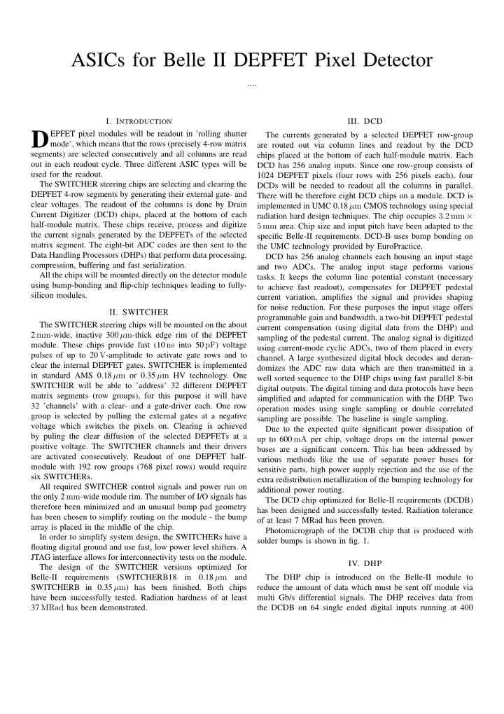
Photomicrograph of the DCDB chip that is produced with solder bumps is shown in fig. 1.
- IV. DHP
The DHP chip is introduced on the Belle-II module to reduce the amount of data which must be sent off module via multi Gb/s differential signals. The DHP receives data from the DCDB on 64 single ended digital inputs running at 400