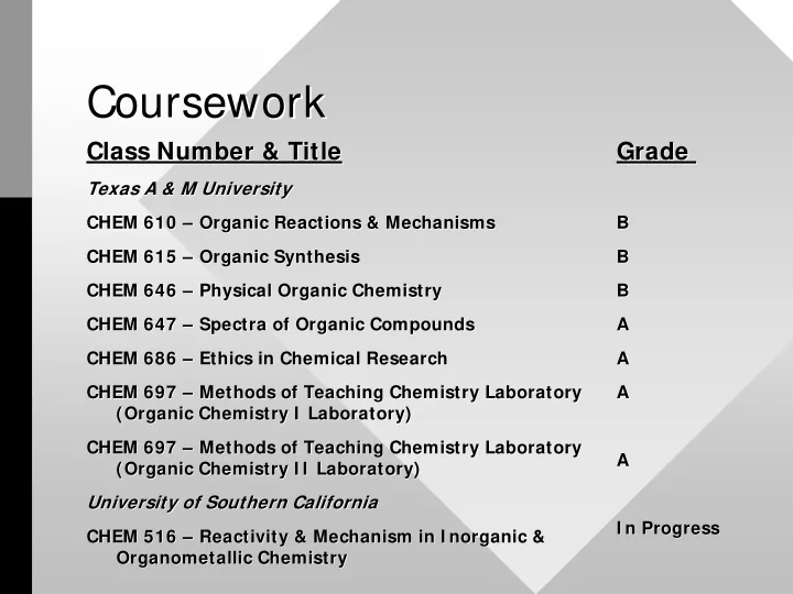

Coursework Coursework
Class Number & Title Class Number & Title
Texas A & M University Texas A & M University CHEM 610 CHEM 610 – – Organic Reactions & Mechanisms Organic Reactions & Mechanisms CHEM 615 CHEM 615 – – Organic Synthesis Organic Synthesis CHEM 646 CHEM 646 – – Physical Organic Chemistry Physical Organic Chemistry CHEM 647 CHEM 647 – – Spectra of Organic Compounds Spectra of Organic Compounds CHEM 686 CHEM 686 – – Ethics in Chemical Research Ethics in Chemical Research CHEM 697 CHEM 697 – – Methods of Teaching Chemistry Laboratory Methods of Teaching Chemistry Laboratory (Organic Chemistry I Laboratory) (Organic Chemistry I Laboratory) CHEM 697 CHEM 697 – – Methods of Teaching Chemistry Laboratory Methods of Teaching Chemistry Laboratory (Organic Chemistry I I Laboratory) (Organic Chemistry I I Laboratory) University of Southern California University of Southern California CHEM 516 CHEM 516 – – Reactivity & Mechanism in I norganic & Reactivity & Mechanism in I norganic & Organometallic Chemistry
Grade Grade
B B B B B B A A A A A A A A I n Progress I n Progress Organometallic Chemistry