coupled inductor as a differential mode noise filter in
play

Coupled Inductor as a Differential Mode Noise Filter in SMPS - PDF document

Coupled Inductor as a Differential Mode Noise Filter in SMPS Sobhika N Sheela S MTech Student, EEE Department Professor, EEE Department NSS College of Engineering, Palakkad NSS College of Engineering, Palakkad Kerala, India Kerala, India


  1. Coupled Inductor as a Differential Mode Noise Filter in SMPS Sobhika N Sheela S MTech Student, EEE Department Professor, EEE Department NSS College of Engineering, Palakkad NSS College of Engineering, Palakkad Kerala, India Kerala, India Sobhika123@gmail.com sheela_unni@yahoo.co.in Abstract — EMI is an issue in Switched Mode Power 
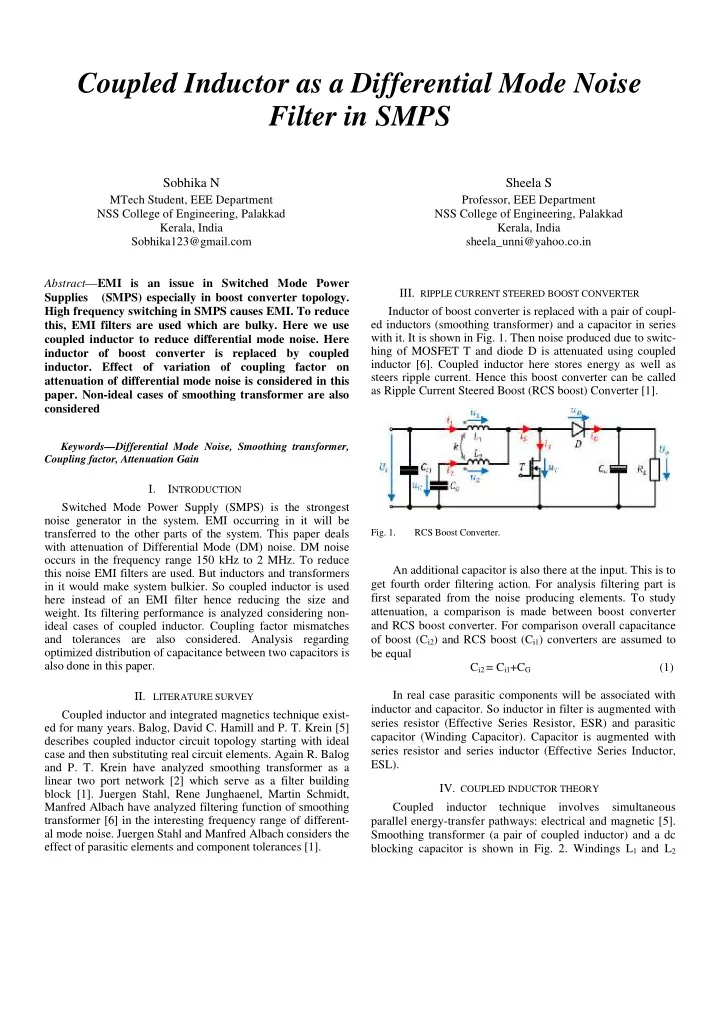
III. RIPPLE CURRENT STEERED BOOST CONVERTER Supplies (SMPS) especially in boost converter topology. High frequency switching in SMPS causes EMI. To reduce Inductor of boost converter is replaced with a pair of coupl- ed inductors (smoothing transformer) and a capacitor in series this, EMI filters are used which are bulky. Here we use with it. It is shown in Fig. 1. Then noise produced due to switc- coupled inductor to reduce differential mode noise. Here hing of MOSFET T and diode D is attenuated using coupled inductor of boost converter is replaced by coupled inductor [6]. Coupled inductor here stores energy as well as inductor. Effect of variation of coupling factor on steers ripple current. Hence this boost converter can be called attenuation of differential mode noise is considered in this as Ripple Current Steered Boost (RCS boost) Converter [1]. paper. Non-ideal cases of smoothing transformer are also considered Keywords—Differential Mode Noise, Smoothing transformer, Coupling factor, Attenuation Gain I. I NTRODUCTION Switched Mode Power Supply (SMPS) is the strongest noise generator in the system. EMI occurring in it will be transferred to the other parts of the system. This paper deals Fig. 1. RCS Boost Converter. with attenuation of Differential Mode (DM) noise. DM noise occurs in the frequency range 150 kHz to 2 MHz. To reduce An additional capacitor is also there at the input. This is to this noise EMI filters are used. But inductors and transformers get fourth order filtering action. For analysis filtering part is in it would make system bulkier. So coupled inductor is used first separated from the noise producing elements. To study here instead of an EMI filter hence reducing the size and attenuation, a comparison is made between boost converter weight. Its filtering performance is analyzed considering non- ideal cases of coupled inductor. Coupling factor mismatches and RCS boost converter. For comparison overall capacitance and tolerances are also considered. Analysis regarding of boost (C i2 ) and RCS boost (C i1 ) converters are assumed to optimized distribution of capacitance between two capacitors is be equal also done in this paper. C i2 = C i1 +C G (1) In real case parasitic components will be associated with II. LITERATURE SURVEY inductor and capacitor. So inductor in filter is augmented with Coupled inductor and integrated magnetics technique exist- series resistor (Effective Series Resistor, ESR) and parasitic ed for many years. Balog, David C. Hamill and P. T. Krein [5] capacitor (Winding Capacitor). Capacitor is augmented with describes coupled inductor circuit topology starting with ideal series resistor and series inductor (Effective Series Inductor, case and then substituting real circuit elements. Again R. Balog ESL). and P. T. Krein have analyzed smoothing transformer as a linear two port network [2] which serve as a filter building IV. COUPLED INDUCTOR THEORY block [1]. Juergen Stahl, Rene Junghaenel, Martin Schmidt, Manfred Albach have analyzed filtering function of smoothing Coupled inductor technique involves simultaneous transformer [6] in the interesting frequency range of different- parallel energy-transfer pathways: electrical and magnetic [5]. al mode noise. Juergen Stahl and Manfred Albach considers the Smoothing transformer (a pair of coupled inductor) and a dc effect of parasitic elements and component tolerances [1]. blocking capacitor is shown in Fig. 2. Windings L 1 and L 2

  2. carries dc and ac currents respectively. When capacitor C G is Effective inductance (L seff ) provided by the smoothing transformer to the boost converter is analyzed to see the ) across it becomes zero [5]. large, ac voltage ( impact of coupling factor. Effective inductance is given by (4) L Seff will be same as L 2 in case of ideal compensation from equation (3). But in real cases, it varies with k for different matching coupling factors k 01 . Sensitivity of L Seff for relative deviation of coupling factor is depicted in Fig. 4. Relative deviation of coupling factor is defined as Fig. 2. Coupled Inductor with capacitor in series with one winding. (5) Then ac voltage across secondary winding L 2 will be transferred to L 1 winding. Now output voltage will have only It can be inferred from Fig. 4 that L Seff is less sensitive to dc component. This is how ideal smoothing transformer steers k 01 in the undercompensation region (K < 0). Effective boost ripple. But zero ripple is not possible in real cases [2]. Because inductance is strongly dependent on coupling factor in overc- capacitor will have a finite value and some ripple would ompensation region (K > 0). We should get perfect compensa- appear at the output port. For analyzing coupled inductor it tion. But manufacturing tolerance may cause inductance value can be represent ed in its equivalent “T” model as in Fig. 3. M to vary. So we always aim for a slight undercompensation is the mutual inductance and can be expressed as region. Inductance values are set accordingly. (2) where is the coupling factor Fig. 4. L Seff versus relative deviation of coupling factor. Fig. 3. Coupled in ductor filter model represented by its equivalent “T” model. A. Effect of parasitic components Coupling factor ranging from 0 < k < 1 is permissible. In First parasitic inductance (ESL) alone is considered. Frequency response of filter for different coupling factor practice, values of k > 0.9 are easily achievable. The operating mismatches (K) are shown in Fig. 5. Dashed line represents regime of coupled inductor is sensitive to coupling factor k [6] filter for boost converter. All others represents filter for RCS which depends on many factors including magnetic flux path boost converter. For comparison, amplitude response of ideal geometry . filter is shown in Fig. 6 for various coupling factor mismatches. In ideal case perfect compensation [5] in L 1 winding is possible for the matching coupling factor . (3) V. SIMULATION AND ANALYSIS Frequency responses of coupled inductor are plotted for ideal and non-ideal cases and analysis is done. With coupling factor equal to k 01 the filter will degenerate into a second order filter with characteristic 40 dB/decade roll off. When coupling factor is less than this value, it results in undercompensation. This can also be called as notch mode. When k > k 01 , it results in overcompensation. This mode of operation is not useful Fig. 5. Amplitude response taking ESL into account. since it gives worse attenuation [2].

  3. Fig. 6. Amplitude response of filter without parasitic components. Fig. 7. Amplitude response taking ESLs and winding capacitances into account. Dashed line represents boost filter and others represent RCS Boost Comparing Fig. 5 and Fig. 6 we can observe that filter. additional resonance appears in Fig. 5. The new additional resonant frequency f res is due to natural resonance of the Positive value of attenuation gain gives good attenuation. capacitors and is given by (8) (6) In Fig. 5 we can see that better filtering obtained in the interesting frequency range for differential mode noise, 150 kHz to 2 MHz. Also we can see that undercompensation performs better in this range compared to ideal and overcompensation. Considering winding capacitances and parasitic inductance another resonance f res4 occurs in the frequency range for DM noise as in Fig. 7. Comparing Fig. 5 and Fig. 7 we can see that this frequency is less than resonant frequency due to parasitic inductance. This resonant frequency f res4 can be calculated as (7) Fig. 8. Amplitude response taking ESL, winding capacitances and parasitic resistors. Though three winding capacitors are there viz C 1 , C 2 , C 12, major influence is due to C 1 . Other two capacitors play minor role. Influence of C 1 at the beginning of the frequency range is minor. Better attenuation is obtained in the range 100 kHz to 1 MHz. Taking parasitic resistors also into account, resonances are damped as seen in Fig. 8. Damping of resonance step-up of first two pole pairs occurs at around 12 kHz and 50 kHz. Only R 1 , R 2 and ESR G have effect on the resonance. Wider frequency band is now obtained where coupled inductor performs better attenuation. B. Attenuation Gain Fig. 9. Amplitude response of attenuation with and without(dashed) Comparison of the two filters (filter for boost converter parasitic elements. and filter for RCS boost converter) can be done with We can see from Fig. 9 that positive attenuation gain is attenuation gain. Attenuation gain, A(s), can be determined obtained from frequency of 150 kHz where the EMI using equation (8). regulations start. Attenuation gain for ideal and non-ideal

Download Presentation
Download Policy: The content available on the website is offered to you 'AS IS' for your personal information and use only. It cannot be commercialized, licensed, or distributed on other websites without prior consent from the author. To download a presentation, simply click this link. If you encounter any difficulties during the download process, it's possible that the publisher has removed the file from their server.

Recommend


More recommend