classical control for quantum
play

Classical Control for Quantum Qubit decoherence Physical - PowerPoint PPT Presentation

Quantum Computing is Hard Classical Control for Quantum Qubit decoherence Physical isolation from environment Computers Error correction correcting error correction! Decoherence-free subspaces Mark Whitney, Nemanja Isailovic,


  1. Quantum Computing is Hard Classical Control for Quantum • Qubit decoherence – Physical isolation from environment Computers – Error correction correcting error correction! – Decoherence-free subspaces Mark Whitney, Nemanja Isailovic, Yatish Patel, John Kubiatowicz U.C. Berkeley Quantum Computing is Harder! 
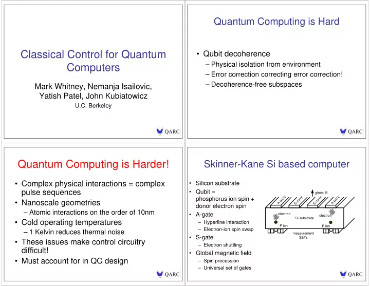
Skinner-Kane Si based computer • Complex physical interactions = complex • Silicon substrate pulse sequences • Qubit = global B E E E E phosphorus ion spin + T T T T A A A A G G • Nanoscale geometries G G A - A - S - S - donor electron spin – Atomic interactions on the order of 10nm • A-gate electron electron Si substrate • Cold operating temperatures – Hyperfine interaction P ion P ion – Electron-ion spin swap – 1 Kelvin reduces thermal noise measurement • S-gate SETs • These issues make control circuitry – Electron shuttling difficult! • Global magnetic field • Must account for in QC design – Spin precession – Universal set of gates

  2. Swap cell Quantum wires . . . . . . S A S A S S A S S A S S S . . . . . . A A A S A S S S S S S S S 4 2 1 0 0 2 1 4 1 4 3 5 5 3 4 1 S S A S S A • Ions are stationary e 1 - e 1 e 1 e 2 e 2 e 1 - - - - - e 2 e 2 e 1 e 1 - - - - e 2 e 1 e 1 e 2 - - - - e 2 e 1 e 1 e 2 e 2 - - - - - e 2 - – Qubits are moved by swapping • Alternating swap gives us “wires” e 2 - e 1 - Electron-ion spin swap – Some qubits move right, some left P ion 1 P ion 2 Electron-ion spin swap • Quantum wires seem more complicated than classical… • A lot of steps for two qubits! Swap Cell Control Pulse Sequence for 2-D Time Step 1 2 3 4 5 6 7 8 9 10 11 12 13 14 S 4 e 2 - e 2 - e 2 - e 2 - e 2 - e 2 - • 2-D layout (mentioned Electrons are too close A 2 e 2 - e 1 - e 2 - e 1 - Electrodes in Kane ’00) moves - - e 1 e 1 S 3 e 2 - S 1 S 2 S 3 e 2 - e 1 - e 1 - electrons in parallel e 1 - e 1 - e 1 - S 2 . . . . . . e 2 - e 2 e 1 - - A 1 A 2 – Simpler control - e 2 - e 2 A 1 e 1 - e 2 - e 2 - e 1 - – Better electron S 3 S 1 S 2 - - e 2 e 2 S 1 e 1 - e 1 - e 1 - e 1 - e 1 - separation e 1 - 24 A 1 24 24 A 1 ,A 2 • Control signals still Control A 2 signals S 1 S 1 complicated! S 2 S 2 – S-gate cascade S 3 S 3 Electron-ion spin swap – A-gate sequence S 4 • What a mess! Long pulse sequence…

  3. Pulse Characteristics Qubit layout • voltage swing (V max ) adjusts d qubit • Clock rate . . . – Tuned for desired error rate – Electron-ion interaction period: • slew rate and clock period adjusts d Si e - 88.3ps -> 11.3GHz clock rate – Lowers electrode to back gate capacitance • Other technologies? (SOI) • Voltage swing • Pulse characteristics effect quantum datapath . . . . . . – Slower qubit manipulation d qubit e - – Lower voltage swing = lower voltage Gate Electrodes V max differential 0V d Si . . . . . . • Slew rate 0V – A-/S-gates must charge in clock period e - Single-electron transistors (SETs) Swap control circuit Control Input • S-/A-gate pulse Tunnel Junction - - e 1 e 1 sequences complex S 1 S 3 S 2 Island e 1 - - e 1 V DD . . . . . . • What would a circuit A 1 A 2 - e 2 - e 2 schematic look like? S 3 S 2 S 1 V DD e 2 - e 2 - C LOAD Y. Takahashi et. al. • CMOS does not work at 1K operating temperature 24 A 1 ,A 2 • SETs work well at low temperatures S 1 • Electrons move 1-by-1 through tunnel junction onto S 2 quantum dot and out other side S 3 • Low drive current (~5nA) and voltage swing (~40mV) – Affects our error and slew rates

  4. Swap control circuit II Large! S 1 on S 1a S 3a S 2 on S 1b S 3b S 1 on S 3 on S 3 on S 1c S 3c A on S 4 on S 1d S 3d A a - - e 1 e 1 S 1 S 3 S 2 • Control circuit area, D D D D D D D S 2a S 4a S 2 on S 4 on - e 1 e 1 - S 2b S 4b . . . . . . S 1a S 2a S 3a S 3b S 4a S 1b ~10um 2 A 1 A 2 S-gate pulse cascade S 3c S 4b - e 2 - S 1c S 1d S 2b S 3d e 2 T – Aggressive process, S 3 S 1 D S 2 D D D D D D D - - e 2 e 2 30nm feature size – Minimal design Reset 24 7 A 1 ,A 2 4 3 2 1 0 • Swap cell area, 6 Reset S 1 5 8-bit counter 4 ~0.068um 2 A a 5-bit counter S 2 3 2 S 3 1 • Will not fit! Enable 0 A-gate pulse repeats 24 times Off-on A-gate pulse subsequence (2 off, 254 on) • Can this even be built with SETs? In SIMD we trust? Why on-chip? • Large control circuit/small swap cell ratio = SIMD • Like clock distribution network • Why not run many wires in from outside? • Clock skew at 11.3GHz? • Error correction • Error correction? complicates . . . . – Requires conditional . Swap . swapping S 3 A S 1 S 3 A S 1 S 2 S 2 Control 1000 qubits S 2 S 2 S 1 S 3 A S 1 S 3 A * 4 signals/qubit in swap S 2 S 2 S 2 S 2 S 1 A S 3 S 1 A S 3 * 336 swaps/lvl 1 ECC S 2 S 2 S 2 S 2 S 1 S 3 A S 1 S 3 = 1344000 wires! A S 2 S 2 1,000,000 wire bus! S 2 S 2 S 1 A S 3 . S 1 A S 3 • ECC could mean trouble . . . for SIMD in general . .

  5. Conclusions • Pulse sequences for quantum gates are complex! • All quantum computing technologies require complex pulse sequences • Must keep control circuit in mind for large- scale integration

Download Presentation
Download Policy: The content available on the website is offered to you 'AS IS' for your personal information and use only. It cannot be commercialized, licensed, or distributed on other websites without prior consent from the author. To download a presentation, simply click this link. If you encounter any difficulties during the download process, it's possible that the publisher has removed the file from their server.

Recommend


More recommend