
SLIDE 1
Chapter 1: The digital abstraction
Computer Structure &
- Intro. to Digital Computers
- Dr. Guy Even
Tel-Aviv Univ.
– p.1
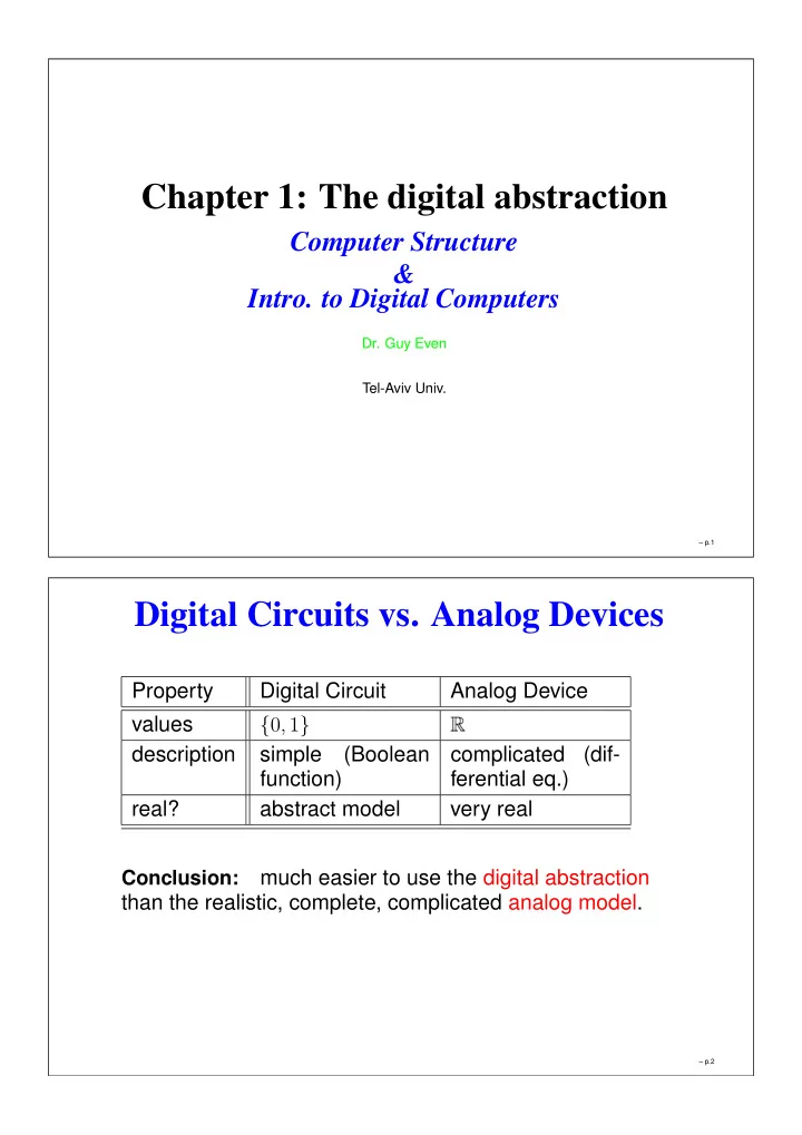
Digital Circuits vs. Analog Devices
Property Digital Circuit Analog Device values
{0, 1}
- description
simple (Boolean function) complicated (dif- ferential eq.) real? abstract model very real
Conclusion:
much easier to use the digital abstraction than the realistic, complete, complicated analog model.
– p.2