
SLIDE 1
Building Chips
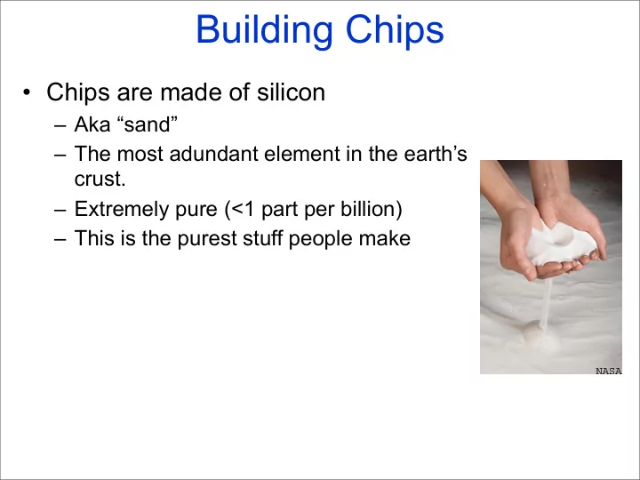
- Chips are made of silicon
Building Chips Chips are made of silicon Aka sand The most - - PowerPoint PPT Presentation
Building Chips Chips are made of silicon Aka sand The most adundant element in the earths crust. Extremely pure (<1 part per billion) This is the purest stuff people make Building Chips Silicon wafers
– To Build a Wire (abridged and simplified) Silicon Wafer
– To Build a Wire (abridged and simplified) Silicon Wafer Silicon Wafer SiO2
Grow silicon dioxide
– To Build a Wire (abridged and simplified) Silicon Wafer Silicon Wafer SiO2
Grow silicon dioxide
Silicon Wafer SiO2 Resist
Apply photo resist
– To Build a Wire (abridged and simplified) Silicon Wafer Silicon Wafer SiO2
Grow silicon dioxide
Silicon Wafer SiO2 Resist
Apply photo resist
Silicon Wafer SiO2 Resist Mask Mask
Expose to UV
– To Build a Wire (abridged and simplified) Silicon Wafer Silicon Wafer SiO2
Grow silicon dioxide
Silicon Wafer SiO2 Resist
Apply photo resist
Silicon Wafer SiO2 Resist Mask Mask
Expose to UV
Silicon Wafer SiO2
Patterned resist
– To Build a Wire (abridged and simplified) Silicon Wafer Silicon Wafer SiO2
Grow silicon dioxide
Silicon Wafer SiO2 Resist
Apply photo resist
Silicon Wafer SiO2 Resist Mask Mask
Expose to UV
Silicon Wafer SiO2
Patterned resist
Silicon Wafer
Etch SiO2
– To Build a Wire (abridged and simplified) Silicon Wafer Silicon Wafer SiO2
Grow silicon dioxide
Silicon Wafer SiO2 Resist
Apply photo resist
Silicon Wafer SiO2 Resist Mask Mask
Expose to UV
Silicon Wafer SiO2
Patterned resist
Silicon Wafer
Etch SiO2
Silicon Wafer Met
Deposit metal
– To Build a Wire (abridged and simplified) Silicon Wafer Silicon Wafer SiO2
Grow silicon dioxide
Silicon Wafer SiO2 Resist
Apply photo resist
Silicon Wafer SiO2 Resist Mask Mask
Expose to UV
Silicon Wafer SiO2
Patterned resist
Silicon Wafer
Etch SiO2
Silicon Wafer Met
Deposit metal
Silicon Wafer Met
Etch SiO2 (Or not)
– Data representation
(electron spin, optical polarization, or volumes of water are also possible). – Computation
– CMOS, Domino logic, current-mode logic, etc.
PMOS NMOS metal
semiconductor Gate V Current Gate V Current
1.8V -- Logic One 0V -- Logic Zero A = 1 Q = 1 A = 0 1 Q = 0 1
Pull-up network Pull-down network
1.8V -- Logic One 0V -- Logic Zero A = 1 Q = 1 A = 0 1 Q = 0 1