
SLIDE 1
1
BACKEND DESIGN Circuit Partitioning
CAD for VLSI 2
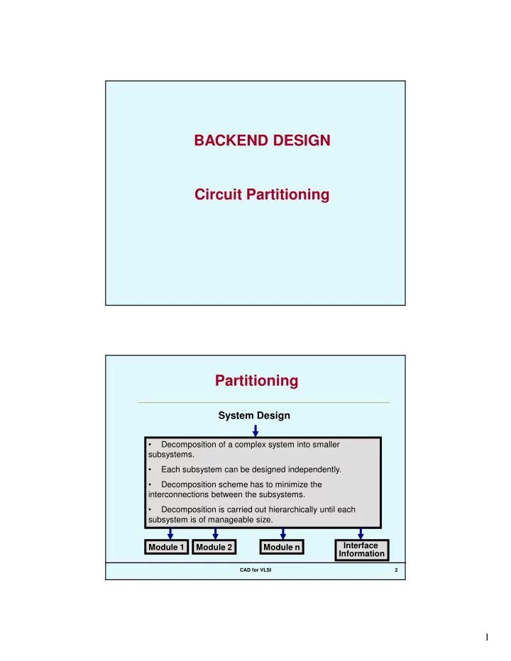
Partitioning
- Decomposition of a complex system into smaller
subsystems.
- Each subsystem can be designed independently.
- Decomposition scheme has to minimize the
interconnections between the subsystems.
- Decomposition is carried out hierarchically until each