Atomic Switch for making new type of electronic devices and systems - - PowerPoint PPT Presentation

Atomic Switch for making new type of electronic devices and systems - - PowerPoint PPT Presentation
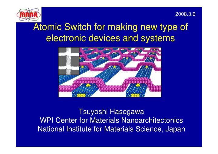
2008.3.6 Atomic Switch for making new type of electronic devices and systems Tsuyoshi Hasegawa WPI Center for Materials Nanoarchitectonics National Institute for Materials Science, Japan Further Progress by Nanotechnology Nanotechnology
Further Progress by Nanotechnology
Performance Year
Transistor 4G DRAM Vacuum Technology Si-electronics Technology
1900 1950 2000 2050
IC LSI VLSI ULSI
Alchemy of 20th c.
Nano-electronics
Nanotechnology driven
Molecular Electronics Spin-Electronics Carbon-Electronics Atomic Electronics Quantum Computing
Key point for the further progress
Miniaturization Using new functions by new materials & new structures Molecules smallest building blocks & Atoms
Atomic Switch
Atomic movement was achieved by electrical field. ON/OFF : 10 OFF ON
W tip Ni Xe
- D. M. Eigler et al., Nature 352 (1991) 600.
OFF ON
- K. Terabe et al., Nature 433 (2005) 47.
Atomic movement was achieved by solid electrochemical reaction. ON/OFF : >103
OUTLINE 1.Mechanism and Characteristics 2.Application for Commercial Devices 3.New Type of Atomic Switch
Small Size and Low On-resistance
OFF ON
Atomic movement is controlled.
Atomic switch OFF ON Semiconductor Switch
Electronic distribution is controlled 1μm 1nm 1k 10 100 10k 1 1mm
GaAs-FET MOSFET
Atomic switch ON resistance(Ω) Switch size
switched on
Ag wire Ag2S Pt e- e- Ag Ag + Ag + e-
+
- Ag Ag + e
+
- Ag + e Ag
+
- +
- Ag
switched off
Operating Mechanism
S2- Ag+
Ag2+δS
200μm
Ag nanowire growth by e-beam Ag2S Crystal
The two electrodes are fixed in the case of atomic switch operation.
Single Ag protrusion growth by STM
200 150 100 50 8000 6000 4000 2000
1: Vs= -2.0V It=0.05nA 2: Vs= -2.0V It=1.35nA 3: Vs=+2.0V It=0.05nA 4: Vs=+2.0V It=0.35nA 1 1 1 1 1 1 3 3 3 3 3 3 2 2 2 4 4 4 Change of tip height (nm) Time (sec.)
- +
sample Ag2S Ag tip Ag sample bias
- K. Terabe, T. Nakayama, T. Hasegawa and M. Aono, J. Appl. Phys., 91 (2002) 10110.
Controlled growth and shrinkage
- 1.5 V
- 2.0 V
- 2.5 V
- 3.0 V
+1.5 V +2.0 V +2.5 V +3.0 V
1 10-1 10-2 10-3 10-4 0.0 0.4 0.8 1.2 1.6 Tunneling current (nA) Rate of change in length of Ag protrusion (nm/sec.)
growth shrink
Growth and Shrinkage speed of Ag
= A exp( ) E – D It kT dt dN
Ag+ Ag2+δS Ag+ Ag E growth Ag+ Ag Dg It
・
shrink Ag+ Ag Ds It
・
Switching time t (s) Switching voltage Vs (V)
Atomic switch using Cu2-δS
Switching time t (s) Switching voltage Vs (V)
Atomic switch using Αg2+δS
: 1MΩ to 12.9 kΩ : 100 k Ω to 12.9 kΩ
Switching time vs. switching voltage
- T. Tamura, T. Hasegawa, K. Terabe, T. Nakayama, T. Sakamoto, H. Sunamura,
- H. Kawaura, S. Hosaka and M. Aono, Jpn. J. Appl. Phys. 45 (2006) L364.
Switching characteristics depend on the materials.
Two types of atomic switch
Ag Ag2S Pt Ag Switch Off Switch On
Initial type of Atomic switch Gapless atomic switch (NanoBridgeTM) Cross-section of NanoBridge
Ti Cu Switch Off Cu Switch On Cu2S
‘with gap’ and ‘without dap’
Cu Pt Cu2S Ta2O5 Applying Voltage Cu Pt Cu+ Cation formation and migration Super-saturation @ Pt electrode Cu Pt Growth toward Cu electrode Cu Pt Metal deposition parallel to electrode Cu Pt Metal Bridge Formation Switch ON
Switching Mechanism
- f gapless atomic switch
Operating Model
OUTLINE 1.Mechanism and Characteristics 2.Application for Commercial Devices 3.New Type of Atomic Switch
50 µm
Cell array Decoder Decoder Sense Amp., Controller, etc.
1k-bit nonvolatile memory
- T. Sakamoto, H. Sunamura, M. Mizuno, H. Kawaura, T. Hasegawa, K. Terabe,
- T. Nakayama and M. Aono, IEEE J. Solid-State Circuits 40 (2005) 168.
Apply to Programmable Devices
Switch size reduces to 1/30, On-resistance reduces to 1/40.
Nowadays Switch
Area = 120F2 On-resistance = 2kΩ New device “Programmable CBIC” is proposed.
- T. Sakamoto, H. Sunamura, M. Mizuno, H. Kawaura, T. Hasegawa, K. Terabe,
- T. Nakayama and M. Aono, IEEE J. Solid-State Circuits 40 (2005) 168.
Atomic Switch
Area = 4F2 On-resistance = 50Ω
F: minimum feature size
It enables many functions by a single chip It enables many functions by a single chip
Conventional FPGA FPGA: Field Programmable Gate Array Programmable CBIC CBIC: Cell Based Integrated Circuit
Logic cell
Programmable CBIC
Chip size: 1/10th, or 10 times larger application Number of programs increases vastly. ・Larger number of fine-grain logic cells ・Size reduction due to the small switches
4x4 crossbar circuit
- T. Sakamoto, et al.,
IEEE J. Solid-State Circuits 40 (2005) 168. INPUT OUTPUT1 10μsec. OUTPUT2 Program 1 Program 2
20 20μ μm m
1.8V 0.18µm CMOS logic
Atomic switch
4 X 4crossbar switch CMOS
Atomic switch
Cu Cu2S
Insulating film Au/Pt/Ti
OUTLINE 1.Mechanism and Characteristics 2.Application for Commercial Devices 3.New Type of Atomic Switch
1) Atomic Switch Array using AAO Template 2) Three terminal Atomic Switch 3) Photon-assisted Atomic Switch
- 1.0
- 0.5
0.0 0.5 1.0
- 1.5
- 1.0
- 0.5
0.0 0.5 1.0 1.5 2.0
Iout(mA) Vin(V) Electrochemical plating Electrochemical sulfurization Ag nanowire array Ag/Ag2S nanowire array Self-made porous-alumina template (~10nm pore)
Ag Ag2S
−
Start
“On” “Off”
Ag2S Ag Ag
(a) (b)
Ag
Ag2S/Ag nanorod and its switching property
d:20 nm
- Ch. Liang, K. Terabe, T. Hasegawa, R. Negishi, T. Tamura and M. Aono, Small 10 (2005) 971.
Atomic switch array using AAO
Removing template
Ag Ag2S
3-terminal Atomic Switch
For more controllability, large current, etc.
+ + + + + + + + + + +
- Cu
Pt
Gate Source Drain
- F. Xie et al., Phys. Rev. Lett., 93, 128303 (2004).
3-terminal Atomic Switch
For more controllability, large current, etc.
Cell phones Digital TV Robot Car