
SLIDE 1
WHAT GRAPHICS PROGRAMERS NEED TO KNOW ABOUT DRAM
ERIK BRUNVAND, NILADRISH CHATTERJEE, DANIEL KOPTA
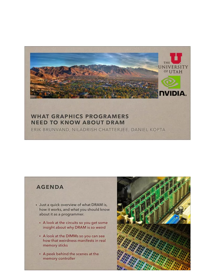
AGENDA
- Just a quick overview of what DRAM is,
how it works, and what you should know about it as a programmer.
- A look at the circuits so you get some
insight about why DRAM is so weird
- A look at the DIMMs so you can see
how that weirdness manifests in real memory sticks
- A peek behind the scenes at the
memory controller