
SLIDE 1
A Vertically Integrated Module Design for Track Triggers at Super-LHC
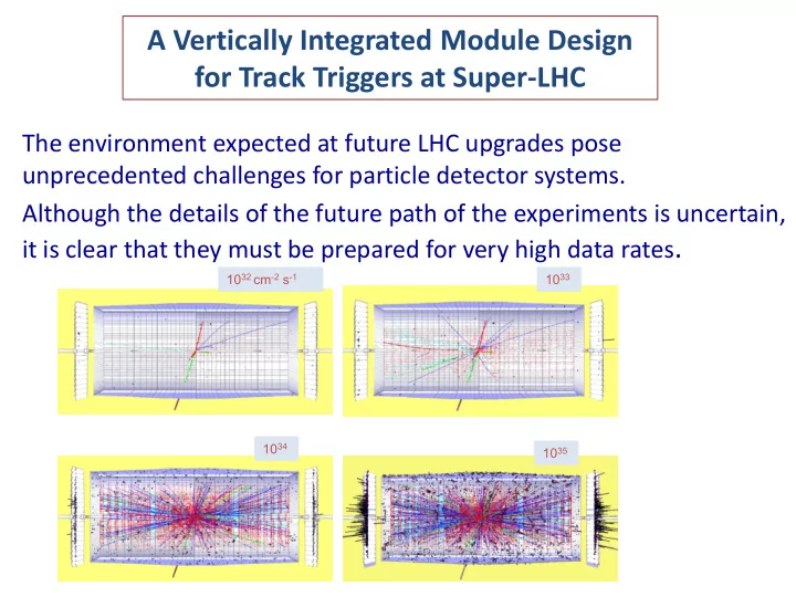
The environment expected at future LHC upgrades pose unprecedented challenges for particle detector systems. Although the details of the future path of the experiments is uncertain, it is clear that they must be prepared for very high data rates.
1033 1033 1035 1035 1032 cm-2 s-1 1032 cm-2 s-1 1034 1034