SLIDE 1
a
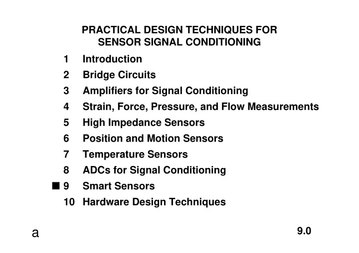
9.0 PRACTICAL DESIGN TECHNIQUES FOR SENSOR SIGNAL CONDITIONING 1 Introduction 2 Bridge Circuits 3 Amplifiers for Signal Conditioning 4 Strain, Force, Pressure, and Flow Measurements 5 High Impedance Sensors 6 Position and Motion Sensors 7 Temperature Sensors 8 ADCs for Signal Conditioning I 9 Smart Sensors 10 Hardware Design Techniques
SLIDE 2 a
9.1 CONTROLLING A REMOTE ACTUATOR USING A 4-20mA LOOP
4-20mA DAC µC HOST COMPUTER REGULATOR LOOP SUPPLY RSENSE
CONTROL ROOM
4-20mA OUTPUT ACTUATOR
AD420
12V TO 32V LOOP RETURN
SLIDE 3 a
9.2 4-20mA LOOP POWERED SMART SENSOR
SENSOR ADC µC 4-20mA DAC RSENSE
AD421
ICOMMON < 4.00mA ADC µC HOST COMPUTER REGULATOR LOOP SUPPLY RSENSE 3.3V / 5V AD7714/AD7715 IAD421 < 0.75mA
CONTROL ROOM
DMOS FET DMOS FET: Supertex DN2535 Siliconix ND2020L or ND2410L 4-20mA RETURN LOOP POWER I µC+SENSOR < 2.75mA I AD7714/AD7715 < 0.50mA ICOMMON
SLIDE 4 a
9.3 HART INTELLIGENT REMOTE TRANSMITTER USING AD421 LOOP-POWERED 4-20mA DAC
SENSOR ADC µC 4-20mA DAC AD421 HART MODEM BELL 202 WAVEFORM SHAPER BANDPASS FILTER LOOP POWER LOOP RETURN CC
HT20C12 / 20C15 (Symbios Logic)
HART DIGITAL SIGNAL: 1200Hz, 2200Hz FREQUENCY SHIFT KEYING (FSK)
SLIDE 5 a
9.4 INDUSTRIAL NETWORKING
NODE
FIELD NETWORK
NODE NODE BRANCH NODE SMART SENSOR SMART SENSOR DEVICE NETWORK SMART SENSOR SMART SENSOR
SLIDE 6
a
9.5 SOME OF THE STANDARDS I Ethernet I Foundation Fieldbus I Lonwork I Profibus I Interbus-S I Universal Serial Bus (USB) I CAN-Bus I Device-Net I WorldFIP I P-NET I HART I ASI
SLIDE 7 a
9.6 THE IEEE 1451.2 SENSOR INTERFACE STANDARD NCAP
FIELD NETWORK - OR - DEVICE NETWORK
TII
STIM
TEDS Sensor
Actuator
I NCAP
= Network Capable Application Processor
I TII
= Transducer Independent Interface
I TEDS
= Transducer Electronic Datasheet
I STIM
= Smart Transducer Interface Module
SLIDE 8 a
9.7 TRUE "PLUG AND PLAY"
Lonwork NCAP Ethernet NCAP Ethernet NCAP
PC with Web Browser
Lonwork NCAP
Ethernet Field Network Lonwork Field Network
Flow Rate STIM Temperature STIM Pressure STIM
SLIDE 9
a
9.8 THE SMART SENSOR Precision Amplifier High Resolution ADC Microcontroller Sensor
Pressure Sensor, RTD, Thermocouple, Strain Gage, etc.
SLIDE 10
a
9.9 THE EVEN SMARTER SENSOR Sensor MicroConverterTM !
Pressure Sensor, RTD, Thermocouple, Strain Gage, etc.
SLIDE 11
a
9.10 THE MicroConverter™
High Performance Analog I/O + On-Chip FLASH Memory + On-Chip Microcontroller
1 2 3 =
MicroConverter™
SLIDE 12
a
9.11 ANALOG I/O 1
I Dual Σ∆ Σ∆ ADC N >16 bit N >100dB SNR (p-p) N Differential Inputs N Prog. Gain Amp N Self-Calibration I 12bit V-Out DAC N < ½ LSB DNL I Voltage Reference I Temperature Sensor I 8 chan SAR ADC N 10 bit N < ½ LSB INL I 12bit V-Out DAC N < ½ LSB DNL I Voltage Reference I Temperature Sensor I 8 chan SAR ADC N 12 bit, 5µs N < ½ LSB INL N DMA mode N Self-Calibration I Dual 12bit V-Out DAC N < ½ LSB DNL I Voltage Reference I Temperature Sensor
ADuC816 ADuC812 ADuC810
SLIDE 13
a
9.12 ON-CHIP FLASH MEMORY 2
I 8K bytes Nonvolatile FLASH Program Memory N Stores Program and Fixed Lookup Tables N In-Circuit Serial Programmable or External Parallel Programmable N Read-Only to Microprocessor Core I 640 bytes Nonvolatile FLASH Data Memory N User “Scratch Pad” for Storing Data During Program Execution N Simple Read / Write Access Through SFR Space I Programming Voltage (VPP) Generated On-Chip
ADuC816 ; ADuC812 ; ADuC810
SLIDE 14
a
9.13 ON-CHIP MICROCONTROLLER 3
I Industry Standard 8052 Core N 12 Clock Machine Cycle w/ up to 16MHz Clock N 32 Digital I/O Pins N Three 16bit Counter/Timers N Universal Asynchronous Receiver/Transmitter (UART) Serial Port I ...Plus Some Useful Extras N SPI or I2C Compatible Serial Interface N WatchDog Timer N Power Supply Monitor N Timer Interval Counter (ADuC816/810)
ADuC816 ; ADuC812 ; ADuC810
SLIDE 15 a
9.14 ADuC816 FUNCTIONAL BLOCK DIAGRAM
AIN MUX AIN MUX buf pga
Σ∆ Σ∆ ADC
ADC control and calibration
Σ∆ Σ∆ ADC
ADC control and calibration
TEMP sensor
2.5V bandgap reference
VREF detect 8K x 8 program FLASH EEPROM 640 x 8 user FLASH
synchronous serial interface
(SPI or I2C) 8052
micro- controller core
256 x 8 user RAM watchdog timer
power supply monitor asynchronous serial port
(UART)
16 bit counter timers timer interval counter OSC & PLL
DAC control
DAC1
buf buf AVDD AGND DVDD DGND SCLK SDATA/ MOSI MISO SS ALE PSEN EA RESET RxD TxD XTAL1 XTAL2 (primary channel) (auxilliary channel) AIN1 AIN2 AIN3 AIN4 VREFIN+ VREFIN– IEXC1 IEXC2 DAC T0 T1 T2 T2EX INT0 INT1 –3.5mV/°C
ADuC816
5 6 20 34 47 21 35 48 26 27 14 13 42 41 40 15 16 17 32 33 43 44 45 46 49 50 51 52 1 2 3 4 9 10 11 12 28 29 30 31 36 37 38 39 16 17 18 19 22 23 24 25 9 10 11 12 8 7 3 4 10 22 23 1 2 18 19 P0.0 P0.1 P0.2 P0.3 P0.4 P0.5 P0.6 P0.7 P1.0 P1.1 P1.2 P1.3 P1.4 P1.5 P1.6 P1.7 P2.0 P2.1 P2.2 P2.3 P2.4 P2.5 P2.6 P2.7 P3.0 P3.1 P3.2 P3.3 P3.4 P3.5 P3.6 P3.7
SLIDE 16 a
9.15 ADuC816 - PRIMARY SPECIFICATIONS
I ADC : INL
SNR (p-p)
- >102dB (17 Noise Free Bits)
Input Range
- ± 20mV to ± 2.56V
- Conv. Rate
- 5.4Hz to 105Hz
I DAC : DNL
Output Range
Settling Time
I Power : Specified for 3V or 5V Operation 5V 3V Normal 7mA 3mA Idle 4.5mA 1.5mA Powerdown <20µA <20µA
SLIDE 17 a
9.16 ADuC812 FUNCTIONAL BLOCK DIAGRAM
AIN MUX
T/H
12-bit ADC
ADC control and calibration
TEMP sensor
2.5V bandgap reference
8K x 8 program FLASH EEPROM 640 x 8 user FLASH
synchronous serial interface
(SPI or I2C) 8052
micro- controller core
256 x 8 user RAM watchdog timer
power supply monitor asynchronous serial port
(UART)
16 bit counter timers OSC
DAC control
DAC1
buf AVDD AGND SCLK SDATA/ MOSI MISO SS ALE PSEN EA RESET RxD TxD XTAL1 XTAL2 ADC0 ADC1 ADC3 ADC4 VREF DAC1 T0 T1 T2 T2EX INT0 INT1 –3.5mV/°C
ADuC812
ADC2 ADC5 ADC6 ADC7 CREF
DAC0
buf DAC0 buf CONVST hardware 43 44 45 46 49 50 51 52 1 2 3 4 11 12 13 14 28 29 30 31 36 37 38 39 16 17 18 19 22 23 24 25 23 5 1 2 3 4 11 12 13 14 8 7 6 20 34 47 21 35 48 26 27 19 12 42 41 40 15 16 17 32 33 9 10 22 23 1 2 18 19 P0.0 P0.1 P0.2 P0.3 P0.4 P0.5 P0.6 P0.7 P1.0 P1.1 P1.2 P1.3 P1.4 P1.5 P1.6 P1.7 P2.0 P2.1 P2.2 P2.3 P2.4 P2.5 P2.6 P2.7 P3.0 P3.1 P3.2 P3.3 P3.4 P3.5 P3.6 P3.7 DVDD DGND
SLIDE 18 a
9.17 ADuC812 - PRIMARY SPECIFICATIONS
I ADC : INL
SNR (p-p)
Input Range
- 0 to VREF
- Conv. Time
- <5µs (200kSPS)
I DAC : DNL
Output Range
Settling Time
I Power : Specified for 3V or 5V Operation 5V 3V Normal 18mA 12mA Idle 10mA 6mA Powerdown <50µA <50µA
SLIDE 19
a
9.18 MicroConverter™ DESIGN SUPPORT
MicroConverterTM Web Site QuickStartTM Development Kit Third Party Development Tools
1 2 3
SLIDE 20
a
9.19 MicroConverter™ WEB SITE
www.analog.com
1
I Data Sheets I Application Notes I 8051 Reference Material I Free Windows MicroConverterTM Simulator I Free Keil ‘C’ Compiler (2K limited version)
SLIDE 21
a
9.20 MicroConverter™ - QuickStart™ DEVELOPMENT KIT
I Documentation
N User’s Guide N Datasheet N Tools Tutorial N Quick Reference Guide
I Evaluation Board
N RS-232 Serial Comms N 32K External SRAM N Buffered Analog I/O
I Regulated Power Supply I Serial Port Cable
I Software
N Metalink Assembler N ‘C’ Compiler (Limited 2K) N Windows Simulator N Serial Downloader N Windows Debugger N Example Code
QuickStartTM
2
SLIDE 22
a
9.21 MicroConverter™ - THIRD PARTY DEVELOPMENT TOOLS
I Keil Compiler N A full function windows based ‘C’ compiler environment featuring a simulator for source and assembly level debugging. I MetaLink Emulator N A high end in circuit emulation system offering a complete windows based environment for in-system debug sessions.
Power Tools
3
All tools will fully integrate with each MicroConverter product The First Two of Many Third Party Tools to Fully Support MicroConverterTM Products:
SLIDE 23 a
9.22 MicroConverter™ PRODUCT ROADMAP
I Larger FLASH Memory Capacity (Data and Program) I Hardware Communications Interface Enhancements (CAN Bus, USB Bus) I Increased Microcontroller Horsepower
TIME
1 ADuC812
12 bit ADC
3 ADuC810
Dual DAC
2 ADuC816
Σ∆ Σ∆ ADC
. . . . Future Products May Include:
. . . .