a molecular description of current flow avik w ghosh
play

A molecular description of current flow Avik W. Ghosh, Kamaram - PDF document

Oral Presentation, Theme F : Molecular and Supramolecular Materials, Organic and Hybrid Electronics ... A molecular description of current flow Avik W. Ghosh, Kamaram Munira and Mikiyas Tsegaye School of Electrical and Computer Engineering,


  1. Oral Presentation, Theme F : Molecular and Supramolecular Materials, Organic and Hybrid Electronics ... A ‘molecular’ description of current flow Avik W. Ghosh, Kamaram Munira and Mikiyas Tsegaye School of Electrical and Computer Engineering, University of Virginia, Charlottesville 22904, USA Abstract — We present a unified formalism for describing current flow through any small 'molecule'. The formalism can be translated into 'first principles' simulations towards predictive properties with no adjustable parameters. Three case studies are presented – electron spectroscopy in buckyballs on silicon, spin currents and torques in an Fe-MgO-Fe tunnel junction, and thermal currents in graphene nanoribbons. In each case, a ‘ molecular ’ description is critical to the underlying physics. Modern day electronics is rapidly reaching nanometer understanding of spintronics is critical to the suitable design of dimensions where atomistic, quantum and many-body effects an STTRAM. An atomistic theory shows that the critical dominate. The non- equilibrium Green’s function (NEGF) switching current can be lowered by selectively filtering the 
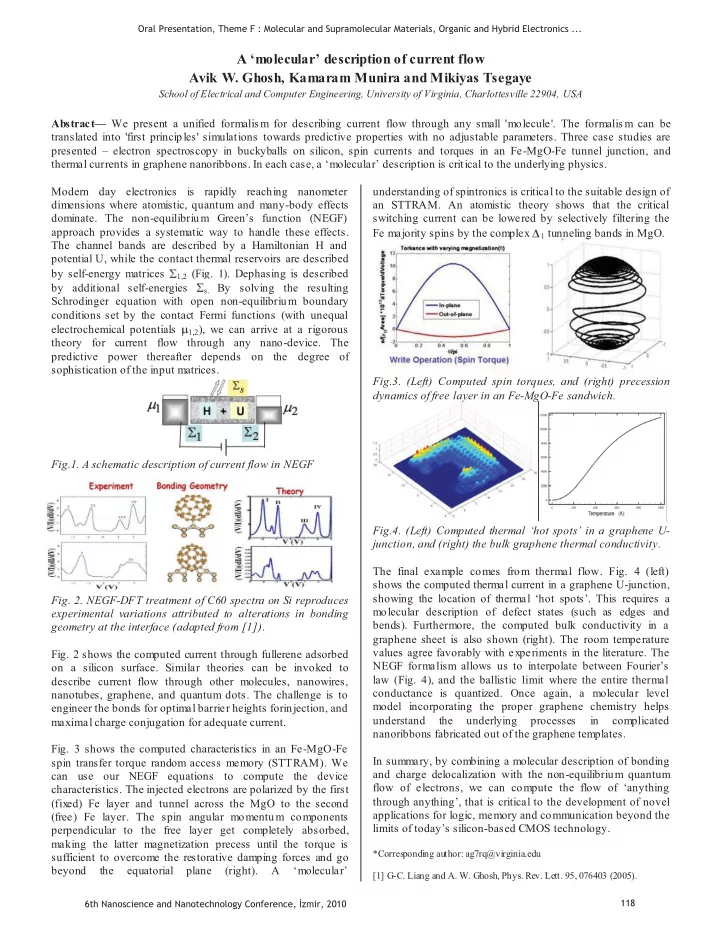
approach provides a systematic way to handle these effects. Fe majority spins by the complex 1 tunneling bands in MgO. The channel bands are described by a Hamiltonian H and potential U, while the contact thermal reservoirs are described by self-energy matrices 1,2 (Fig. 1). Dephasing is described by additional self-energies s. By solving the resulting Schrodinger equation with open non-equilibrium boundary conditions set by the contact Fermi functions (with unequal electrochemical potentials 1,2 ), we can arrive at a rigorous theory for current flow through any nano-device. The predictive power thereafter depends on the degree of sophistication of the input matrices. Fig.3. (Left) Computed spin torques, and (right) precession dynamics of free layer in an Fe-MgO-Fe sandwich. Fig.1. A schematic description of current flow in NEGF Fig.4. (Left) Computed thermal ‘hot spots’ in a gr aphene U- junction, and (right) the bulk graphene thermal conductivity. The final example comes from thermal flow. Fig. 4 (left) shows the computed thermal current in a graphene U-junction, showing the location of thermal ‘hot spots’. This requires a Fig. 2. NEGF-DFT treatment of C60 spectra on Si reproduces molecular description of defect states (such as edges and experimental variations attributed to alterations in bonding bends). Furthermore, the computed bulk conductivity in a geometry at the interface (adapted from [1]). graphene sheet is also shown (right). The room temperature values agree favorably with experiments in the literature. The Fig. 2 shows the computed current through fullerene adsorbed NEGF formalism allows us to interpolate between Fourier’s on a silicon surface. Similar theories can be invoked to law (Fig. 4), and the ballistic limit where the entire thermal describe current flow through other molecules, nanowires, conductance is quantized. Once again, a molecular level nanotubes, graphene, and quantum dots. The challenge is to model incorporating the proper graphene chemistry helps engineer the bonds for optimal barrier heights forinjection, and understand the underlying processes in complicated maximal charge conjugation for adequate current. nanoribbons fabricated out of the graphene templates. Fig. 3 shows the computed characteristics in an Fe-MgO-Fe In summary, by combining a molecular description of bonding spin transfer torque random access memory (STTRAM). We and charge delocalization with the non-equilibrium quantum can use our NEGF equations to compute the device flow of electrons, we can compute the flow of ‘anything characteristics. The injected electrons are polarized by the first through anything’ , that is critical to the development of novel (fixed) Fe layer and tunnel across the MgO to the second applications for logic, memory and communication beyond the (free) Fe layer. The spin angular momentum components limits of today’s silicon -based CMOS technology. perpendicular to the free layer get completely absorbed, making the latter magnetization precess until the torque is *Corresponding author: ag7rq@virginia.edu sufficient to overcome the restorative damping forces and go beyond the equatorial plane (right). A ‘ molecular ’ [1] G-C. Liang and A. W. Ghosh, Phys. Rev. Lett. 95, 076403 (2005). 118 6th Nanoscience and Nanotechnology Conference, �zmir, 2010

Download Presentation
Download Policy: The content available on the website is offered to you 'AS IS' for your personal information and use only. It cannot be commercialized, licensed, or distributed on other websites without prior consent from the author. To download a presentation, simply click this link. If you encounter any difficulties during the download process, it's possible that the publisher has removed the file from their server.

Recommend


More recommend