
SLIDE 1
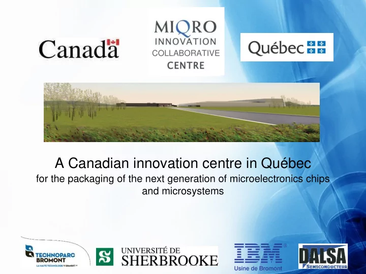
A Canadian innovation centre in Québec
for the packaging of the next generation of microelectronics chips and microsystems
COLLABORATIVE
A Canadian innovation centre in Qubec for the packaging of the next - - PowerPoint PPT Presentation
COLLABORATIVE A Canadian innovation centre in Qubec for the packaging of the next generation of microelectronics chips and microsystems Telecommunications Environment Sensors Power Microelectronics Defense Health care Energy Aerospace
for the packaging of the next generation of microelectronics chips and microsystems
COLLABORATIVE
Defense Aerospace Telecommunications Environment Sensors Health care Transport Power Energy Microelectronics
Internet – Every time anybody sends a request for information on the Internet,
fastest route. Video games – Console video games rely on powerful microchips to compute images. Aerospace – When the defence industry needs to develop the next generation of equipment, microchips will be at the core of the capabilities. Health – Sophisticated medical scans are powered by Canada microchips to render images. Environment – Canada microchips enable computations behind the predictions for climate change and prediction of natural disasters in the Barcelona Supercomputing Center.
When Rover and Pathfinder sent images from Mars, the image sensor systems relied on microchips to render the images. Automotive – In today's new cars, sensors powered by Canada microchips monitor vital functionning ranging from tire pressure to fuel injection system.
Semiconductor, IEDM Conference, Dec. 2006
– Power supply and thermal dissipation are severely challenged – The solutions are both exotic and tailored to the problem
–
New dielectric material (porous and fragile)
–
Materials’ properties a real issue
–
Mechanical integrity is critical
– Need new materials – Require the development of 3 dimensional and optoelectronic solutions – Need faster access time to data
Albany Molecular Research Global Research Burlington Fishkill Poughkeepsie Albany Niskayuna Waterbury Sherbrooke Bromont
– From immediate industrial applications to the exploration of disruptive technologies
– 3 500 engineers, researchers and academics on site
– Dynamics of networks and collaborations linked to centres of excellence reinforce the effectiveness of Minatec
– 4 billion Euros invested over the last 10 years by the microelectronics players in Grenoble-Isère
– Powerful local workforce 13 350 microelectronics professionals
– IBM, Toshiba, AMD, Freescale, STMicroelectronics, Infineon and Samsung, in partnership with University of Albany
complementary and focused on assembly, advanced packaging and test of new microchips
and world class research institutions
Positioning Canada in the global high tech economy:
Leading edge microelectronics:
Building on an existing coalition:
A magnet to
A partnership
5 1 2 3 4
COLLABORATIVE
and equipment manufacturers
Cluster
– Technology crossroads/showcase – 250 specialized scientific jobs – Retention and development of HQP – Scholarships and internships – Visiting international researchers
– Clean rooms: ~60 000 ft2 – Space reserved for incubation
– University-industry partnerships
– Emergence of new companies
– Consolidation of industrial leadership
– Pre-concept, construction and processes coming online by end 2011
COLLABORATIVE
MEMS Future partners Packaging of microchips Laboratories
Canadian Universities Research institutions and Associations International centres Equipment manufacturers Industrials Private R&D centres Private R&D centres
Funding for collaborative projects
COLLABORATIVE
manufacturing processes of: MEMS, 3D Wafer Level Packaging, High Voltage CMOS, CCD Image Sensors, and Analog Mixed Signal CMOS
MEMS pure play foundries in the world
loaded a $100M operation the majority of which is exported to US, Europe and Asia
digital camera, medical, industrial, and aerospace markets.
Manufacturiers et Exportateurs du Canada.
Commerce du Québec
and packaging Inspection Technologies
lithography (45-32-22 nm)
thermal dissipation, carrier design…
processes for 200mm (integrated) MEMS & 3D WLP
patents including ~35 in the MEMS/3D-WLP field
$5.5M/year local business
semiconductor foundry” in Canada.
business is a growth driver for the company
as one of the top three “Pure Play” MEMS foundries – 500M$ market with 30% CAGR
electronics interact with
actuating) and the MEMS revolution has a seed in Bromont
– Pressure sensors, accelerometers, rollover detectors
– Micro fluidics, pressure sensors
– Cell Phones: Motion sensing gyros & Accelerometers, Microphones, RF components – Printers: Ink jet heads – Game console: Motion sensing Gyros & Accelerometers – PC: Microphones – GPS: Motion sensing Gyros & Accelerometers
– Lab on a chip – Gas detection
An increasing number of cell phones incorporate MEMS microphone, speakers, and gyros
MEMS MARKET FORECAST 2007 – 20121
(IN MILLIONS)
Motion sensors are revolutionizing the world of cell phones, GPS, game consoles, cars, etc… MEMS microphones are making their way in cell phones and PC
DEVELOPMENT OF NEW MATERIALS AND PROCESSES – Advanced Photopolymers:
micromachining processes
current and novel thick polymer layers on various films
coating, exposure, develop) needed for plating and regular coat exposure and developing can also be used as a structural material
date indicates very slow, one wafer at a time, process times). Unacceptable for a business. Develop new approaches to quicken the process.
technologies) to accommodate cavity filling, conformal coating requirements
(within wafer) and WTW (wafer to wafer) thickness, RI, and stress variation
etc.)
quartzware cleaning system (quartz tube, liner, boats etc) without etching quartz while etching LSN for cleaning of quartzware
– Low-stress Doped Silicon:
synthesizing low-stress doped silicon thin films
detail in order to optimize the deposition process or to develop new approaches
for achieving high quality deep trenches and explore novel approaches
trench formation including:
– Strip and cleaning trenches – Low-stress nitride development – Stress balanced trenches – Electrical isolation testing – Hermiticity testing – Etchback process characterization
recipes and perform electromechanical reliability tests
technologies such as plasma-activated bonding, solder bonding, eutectic bonding and thermo-compression bonding to ensure flexible technologies for complex wafer-level devices integration, such as integrated MEMS, hermetic WLP, and 3D interconnects.
furnaces
with associated cleaning tools
EQUIPMENT SET FOR MEMS R&D