SLIDE 1
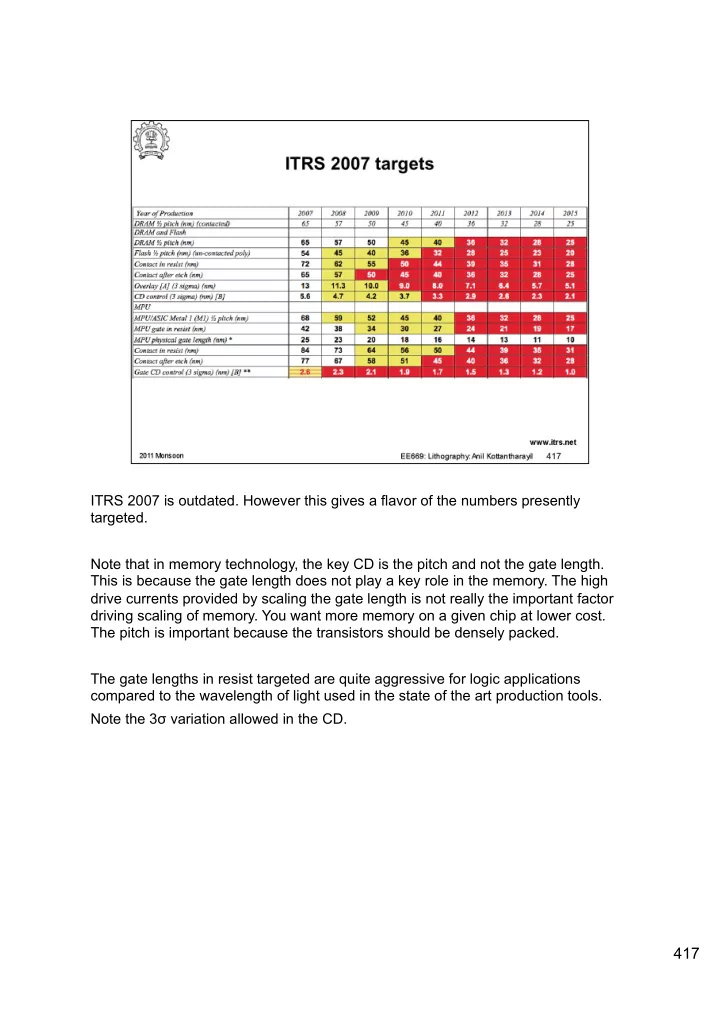
ITRS 2007 is outdated. However this gives a flavor of the numbers presently targeted. Note that in memory technology, the key CD is the pitch and not the gate length. This is because the gate length does not play a key role in the memory. The high drive currents provided by scaling the gate length is not really the important factor driving scaling of memory. You want more memory on a given chip at lower cost. The pitch is important because the transistors should be densely packed. The gate lengths in resist targeted are quite aggressive for logic applications compared to the wavelength of light used in the state of the art production tools. Note the 3σ variation allowed in the CD.
417
SLIDE 2
What is the real meaning of DOF?
418
SLIDE 3
419
SLIDE 4 Modulation transfer function is a measure of the contrast in the image. Lower the MTF, lower is the contrast. Lower contrast is due to diffraction at the edges of the
- features. It may be noted that the MTF for smaller structures that are densely
packed would be smaller. There would be a minimum contrast required for registering the image on the resist. This would then determine the smallest features that can be printed.
420
SLIDE 5 By now you may come to appreciate that the photo resist would play an important role in deciding the desirable end result of lithography. We will not get into the details of the photo resist chemistry. The end result of lithography depends on the application. Let us say small CD is the most important requirement for the specific application. One of the important parameter for lithography is the response of the resist to the amount of light incident
- n it. Here we refer to the light to which the resist would be sensitive. As the light
passes through the resist, it would be absorbed and this would result in some transformation of the resist. The intensity of the light would then reduce. So the top part may be fully transformed whereas the bottom part may not have gone through any transformation. So a minimum amount of light energy should fall on the resist for fully exposing the light. If we do an experiment where in the energy incident per unit area (dose) is varied and the resist is subsequently developed, we would be able to determine the thickness of the resist remaining as a function of dose. In the case of a positive resist, no resist would be developed till a certain dose, Q0 is reached and subsequently the thickness of the remaining resist decreases. The resist would be fully developed when the dose is beyond Qf. The slope of the curve as defined on the slide is the contrast of the resist. Suppose the slope is infinite. That means the response of the resist vis-à-vis the dose is binary, i.e. beyond a threshold dose, the whole resist would be developed. Such a response is desirable if sharp vertical features are desirable in resists.
421
SLIDE 6
These are resist contrast curves for two resists obtained in our lab. Both a electron beam resists. So the dose is the total charges deposited on the resist per unit area. An important thing to note is that the resist would go through several processes before exposure and all of them can have an impact on the contrast. Also resists have low shelf life. So the contrast numbers would indicate the properties of the resist as well as process conditions.
422
SLIDE 7
The importance of the resist contrast curve and MTF can be understood using the figures above. For the feature with smaller MTF, the resist contrast would result in a sloped side wall profile of the resist. The sidewall profile may not be acceptable in some applications.
423
SLIDE 8
424
SLIDE 9
425
SLIDE 10 Light that is incident on the resist may pass through the resist without being
- absorbed. The transmitted light may then be reflected from the surface of the
underlying layer. The reflection can be in various directions depending on the topography on the surface and the refractive indices. One consequence of this is that the light would essentially spread laterally and this would reduce the size of the image on the resist. Light reflected at zero angle to the normal may improve the apparent resist contrast. However the wafer surface would develop topographies during processing and hence the exposure can become locally uneven if excessive reflections exist. So reflections must be reduced in advanced lithography
- processes. An anti reflective coating (ARC) is usually used in such cases. ARC is
spin coated on the surface prior to coating of resist. An extreme case when all the conditions are satisfied may lead to standing wave patterns in the resist leading to regular roughness of the resist edges as shown in the SEM image on the right.
426
SLIDE 11 427
As the feature sizes are reduced, the diffraction effects would result in distortion of images printed and subsequently etched on wafers. The left side shows the design
- n the mask (two levels) and the right side shows the features etched on the wafer.
Both the active areas and gate areas are considerably distorted. One of the key reason is the low resolution of the system due to the loss of highly diffracted light. This would happen from the sharpest edges of the mask.
SLIDE 12
428
This can be corrected to some extent using what is called OPC. You add features to your design to counter the distortions from diffraction. You may appreciate that adding OPC to masks could be a tedious process.
SLIDE 13
429
There can be a design solution as well as shown in this figure. The last figure on the right shows the same design as in the middle. You may note that all the lines are drawn straight without bends. Although this may lead to an overhead of 59% larger area, may be worth considering for critical parts of the design.
SLIDE 14 430
Another option is to improve MTF and hence resolution is to use what is called phase shift mask. The masks we discussed so far may be called binary masks in
- retrospect. They had only transparent regions and opaque regions. In a phase shift
masks, every alternate transparent region is coated with a material which would introduce a phase shift of 180 deg to the light passing through it. As can appreciated from the figure, the MTF would improve significantly in such a scenario. Phase shift masks would be significantly more difficult to design and would be also expensive.
SLIDE 15
If you recollect the ITRS 2007 tables, the pitch (feature size + spacing between features) was in the range of 130nm and some of these technologies are being realized using 193 nm lithography. Since the pitch is less than the wavelength of light used, one of the techniques illustrated in the figures on the slide are used for doubling the pattern density.
431