
SLIDE 1
ALU
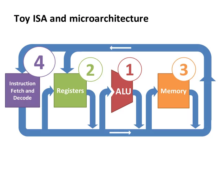
Toy ISA and microarchitecture
Registers Memory
Instruction Fetch and Decode
4 1 3 2 Instruction ALU Registers Memory Fetch and Decode - - PowerPoint PPT Presentation
Toy ISA and microarchitecture 4 1 3 2 Instruction ALU Registers Memory Fetch and Decode Instruction Set Architecture (HW/SW Interface ) processor memory Instructions Instruction Encoded Names, Encodings Logic Instructions
Instruction Fetch and Decode
Instruction Logic Registers
Encoded Instructions Data Instructions
Local storage
Large storage
3
Address Contents First instruction, low-order byte 1 First instruction, high-order byte 2 Second instruction, low-order byte ... ...
(a.k.a. Mini-MIPS)
4
Mnemonic Meaning Opcode Rs Rt Rd ADD Rs, Rt, Rd R[d] ß R[s] + R[t] 0010 s t d SUB Rs, Rt, Rd R[d] ß R[s] - R[t] 0011 s t d AND Rs, Rt, Rd R[d] ß R[s] & R[t] 0100 s t d OR Rs, Rt, Rd R[d] ß R[s] | R[t] 0101 s t d LW Rt, offset(Rs) R[t] ß M[R[s] + offset] 0000 s t
SW Rt, offset(Rs) M[R[s] + offset] ß R[t] 0001 s t
BEQ Rs, Rt, offset If R[s] == R[t] then [PC] ß [PC]+2 + offset*2 Else [PC] ß [PC]+2 0111 s t
JMP offset [PC] ß offset*2 1000
f s e t
(R = register file, M = memory) LSB MSB
5
6
7
8
Instruction
Write Data Read Addr 1 Read Addr 2 Write Addr Read Data 1 Read Data 2
ALU control Write Enable
zero
Control Unit
16 16 16
16 4 4 4 4 Op Rs Rt Rd
9
10
Data Memory
Address Write Data Read Data MemWrite 32 16
Inst
Write Data Read Addr 1 Read Addr 2 Write Addr Read Data 1 Read Data 2
ALU control Write Enable Control Unit
16 16 16
16 4 4 4 4 Sign extend 16 4
How can we support arithmetic and memory instructions? What's shared?
Op Rs Rt Rt Rd (offset)
11
Data Memory
Address Write Data Read Data MemWrite 32 16
Inst
Write Data Read Addr 1 Read Addr 2 Write Addr Read Data 1 Read Data 2
ALU control Write Enable Control Unit
16 16 16
16 4 4 4 4 MUX
MUX MUX
Sign extend 16 4
Mem Op
Op Rs Rt Rd Rd (offset) Rt
12
Op Rs Rt Rd 0111 0001 0010 1110
13
Inst
32 16 Write Data Read Addr 1 Read Addr 2 Write Addr Read Data 1 Read Data 2
ALU
ALU control
Write Enable
Control Unit
16
16
Register File
16 4 4 4 4
MUX MUX
Sign extend 16 4
Read Address Instruction Memory
PC
2 Shift left by 1
+
14
Inst
32 16 Write Data Read Addr 1 Read Addr 2 Write Addr Read Data 1 Read Data 2
ALU
ALU control
Write Enable
Control Unit
16
16
Register File
16 4 4 4 4
MUX MUX
Sign extend 16 4
Read Address Instruction Memory
PC
2 Shift left by 1
+
MUX
Branch?
15
Inst
Data Memory
Address Write Data Read Data MemWrite 32 16 Write Data Read Addr 1 Read Addr 2 Write Addr Read Data 1 Read Data 2
ALU
ALU control
Write Enable
Control Unit
16 16
16
Register File
16 4 4 4 4 MUX
MUX MUX
Sign extend 16 4
Read Address Instruction Memory
PC
2 Shift left by 1
+
MUX
Branch?
16