zyxwvutsrqponmlkjihgfedcbaZYXWVUTSRQPONMLKJIHGFEDCBA Baratunde Cola - PowerPoint PPT Presentation
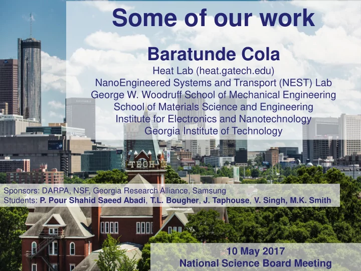
Some of our work zyxwvutsrqponmlkjihgfedcbaZYXWVUTSRQPONMLKJIHGFEDCBA Baratunde Cola Heat Lab (heat.gatech.edu) NanoEngineered Systems and Transport (NEST) Lab George W. Woodruff School of Mechanical Engineering School of Materials Science and
Some of our work zyxwvutsrqponmlkjihgfedcbaZYXWVUTSRQPONMLKJIHGFEDCBA Baratunde Cola Heat Lab (heat.gatech.edu) NanoEngineered Systems and Transport (NEST) Lab George W. Woodruff School of Mechanical Engineering School of Materials Science and Engineering Institute for Electronics and Nanotechnology Georgia Institute of Technology Sponsors: DARPA, NSF, Georgia Research Alliance, Samsung Students: P. Pour Shahid Saeed Abadi , T.L. Bougher , J. Taphouse , V. Singh, M.K. Smith 10 May 2017 National Science Board Meeting
Carbon nanotubes (CNT) 20 μm Technology - Highlights • High thermal conductivity • Billions of aligned nanoscale thermal paths Aluminum foil (layer) • Demonstrated >30% improvement over alternative solutions Carbon nanotubes (CNT) For private discussions only. Company proprietary and confidential
Real interface ‘ Ideal ’ interface zyxwvutsrqponmlkjihgfedcbaZYXWVUTSRQPONMLKJIHGFEDCBA Solid 2 Solid 2 Filler k → ∞ material Solid 1 Solid 1 Gas gap Characteristics desired for thermal interface materials • High thermal conductivity • High conformability • Chemically and mechanically robust in diverse environments zyxwvutsrqponmlkjihgfedcbaZYXWVUTSRQPONMLKJIHGFEDCBA • Major challenge: soft materials with high thermal conductivity are rare in nature Slide 3 Bara Cola 5/8/2017
zyxwvutsrqponmlkjihgfedcbaZYXWVUTSRQPONMLKJIHGFEDCBA zyxwvutsrqponmlkjihgfedcbaZYXWVUTSRQPONMLKJIHGFEDCBA Resolving CNT Interfaces: One-Sided • Resolution enabled by photoacoustic thermal measurement B.A. Cola et al., J. Appl. Phys. 101 , 054313 (2007) copper copper Ag 10 µ m 10 µ m silicon Si silicon Slide 4 Bara Cola 5/8/2017
Wax coated CNTs Gold coated CNTs zyxwvutsrqponmlkjihgfedcbaZYXWVUTSRQPONMLKJIHGFEDCBA 5 µm ~100% resistance reductions B.A. Cola et al., ASME S ummer Heat Transfer Conference 2008 R. Cross et al., Nanotechnology , (2010) with each approach, but reliability and scalability Sprayed on Polymer Bondi ng continues to improve Desi gner Surface Modifiers Growth substrate Bonding substrate EtO Si Br , rt P OEt EtO i) 130 °C ii) MeOH: H 2 O (20:1), rt I HO P O EtO P O OEt OH J.H. Taphouse et al., Nanotechnology, 24 :105401, 2013 J.H. Taphouse et al., Advanced Functional Materials , 2014 Collaboration with organic chemist Dr. Seth Marder (GT) Slide 5 Bara Cola 5/8/2017
CORPORATION Funding to date: >$2 million grants $1.4 million in angel and VC funds
First Thermally Conductive Amorphous Polymer RE S E A RC H SC A LE PRO TO Y PE zyxwvutsrqponmlkjihgfedcbaZYXWVUTSRQPONMLKJIHGFEDCBA V. Sing h, e t a l. Nat Nano te c no l (5), 2014
DVR BOX PLA STIC S FO R C O O LER ELEC TRO NIC S CE L L PHONE Sta nda rd T CPo ly Pla stic Pla stic Ma x: 74 ° C Ma x: 48 ° C L E D BUL B
Rectifying Antenna or ‘Rectenna’ Microwave rectenna Solar rectenna (born 1963, Raytheon and Purdue) (proposed 1972) Demonstrated efficiencies > 80% Predicted efficiencies > 80% Slide 9 Bara Cola 5/8/2017
Rectification Physics (Classical) Cutoff frequency Diode resistance V t e - Diode Junction Diode responsivity V t Antenna EM field Rectenna voltage and power output Slide 10 Bara Cola 5/8/2017
MWCNT Rectenna: Structural Detail • 8 nm conformal alumina coating • CNT tip field enhancement • ~ 10 nm junction diameter (C~1 aF) • Ca/Al low work function top contact (semi-transparent, ~10% transmission) T op me tal ~ 6 CNT walls Al 2 O 3 c oate d CNT s zyxwvutsrqponmlkjihgfedcbaZYXWVUTSRQPONMLKJIHGFEDCBA 10 nm 1 µm 100 nm Slide 11 Bara Cola 5/8/2017
How the Tunneling Diode Works e - F E φ M’ - e φ CNT φ CNT E F φ M’ φ CNT e - ’ ’ ’ E F E E φ M’ E F F F MWCNT E F tunneling diode Afte r c o nta c t F o rwa rd b ia s Re ve rse b ia s ~ 5 ev MWCNT work function 2.9 ev WF 4.3 ev WF Slide 12 Bara Cola 5/8/2017
Device Capacitance Length and time scale for rectification cutoff frequency is different from length and time scale of device operation! Fermi velocity < 10 6 m/s, so R ( t≈10 -15 s) = ∞ R (t) R (t) Slide 13 Bara Cola 5/8/2017
Impedance Matching Poor impedance matching in a single junction is compensated by larger number of junctions, which allows power production. Phys. Rev. B 87, 161401(R), 2013 Collective antenna effects reduce coupling resistance to single CNT antenna. R (t) R (t) Collective CNT antenna array – approximately in phase Slide 14 Bara Cola 5/8/2017
Rectification Photoresponse Predicted physics J. Phys. D: Appl. Phys. 46 (2013) 135106 Slide 15 Bara Cola 5/8/2017
Recommend
More recommend
Explore More Topics
Stay informed with curated content and fresh updates.





![From: Sherry Ridout [mailto:s.ridout@shaw.ca] Sent: June 14, 2015 10:25 PM To: 'Katharina Gustavs'](https://c.sambuz.com/78542/from-sherry-ridout-mailto-s-ridout-shaw-ca-sent-june-14-s.webp)
